Metal-Gated MOSFET Devices Having Scaled Gate Stack Thickness

a metal-gated mosfet and gate stack technology, which is applied in the direction of semiconductor devices, electrical devices, transistors, etc., can solve the problems of regrowth of interfacial oxide regions, negative affecting device performance, and thickness limitation, and achieve the effect of improving performan

Inactive Publication Date: 2009-04-30
GLOBALFOUNDRIES INC
View PDF23 Cites 43 Cited by
  • Summary
  • Abstract
  • Description
  • Claims
  • Application Information

AI Technical Summary

Benefits of technology

[0007]The present invention provides metal-oxide semiconductor field effect transistor (MOSFET) devices having metal gate stacks and techniques for improving performance thereof. In one aspect of the invention, a metal-oxide semiconductor device is provided comprising a substrate having a buried oxide la

Problems solved by technology

However, regrowth of the interfacial oxide region, e.g., during fabrication of the device, can negatively affect device performance, as it increases the effective oxide thickness (EOT) and degrades the short channel and scaling benefits of the metal gate.
Having a thicker metal gate

Method used


Image

  • Metal-Gated MOSFET Devices Having Scaled Gate Stack Thickness
  • Metal-Gated MOSFET Devices Having Scaled Gate Stack Thickness
  • Metal-Gated MOSFET Devices Having Scaled Gate Stack Thickness

Examples


Embodiment Construction

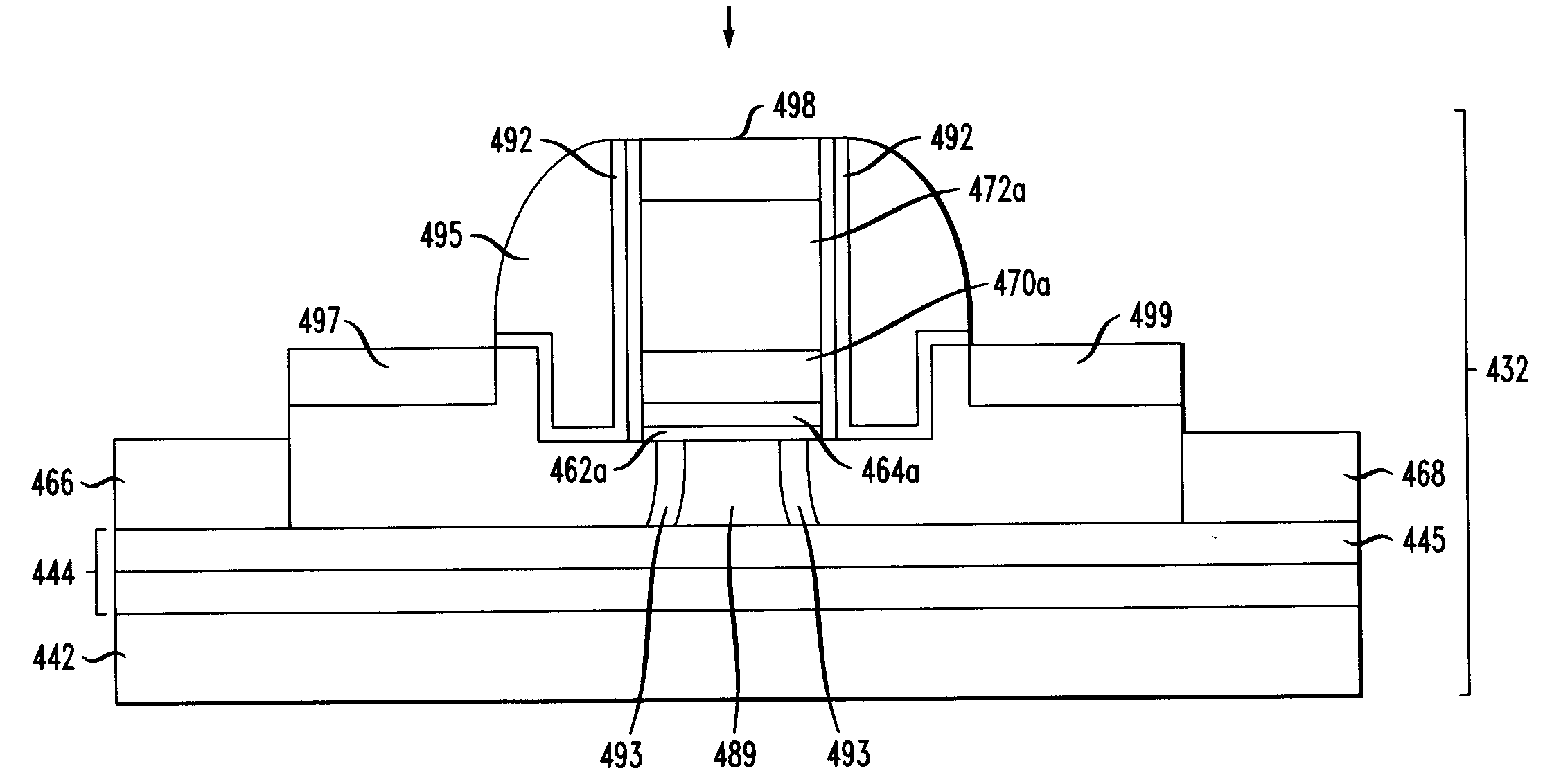
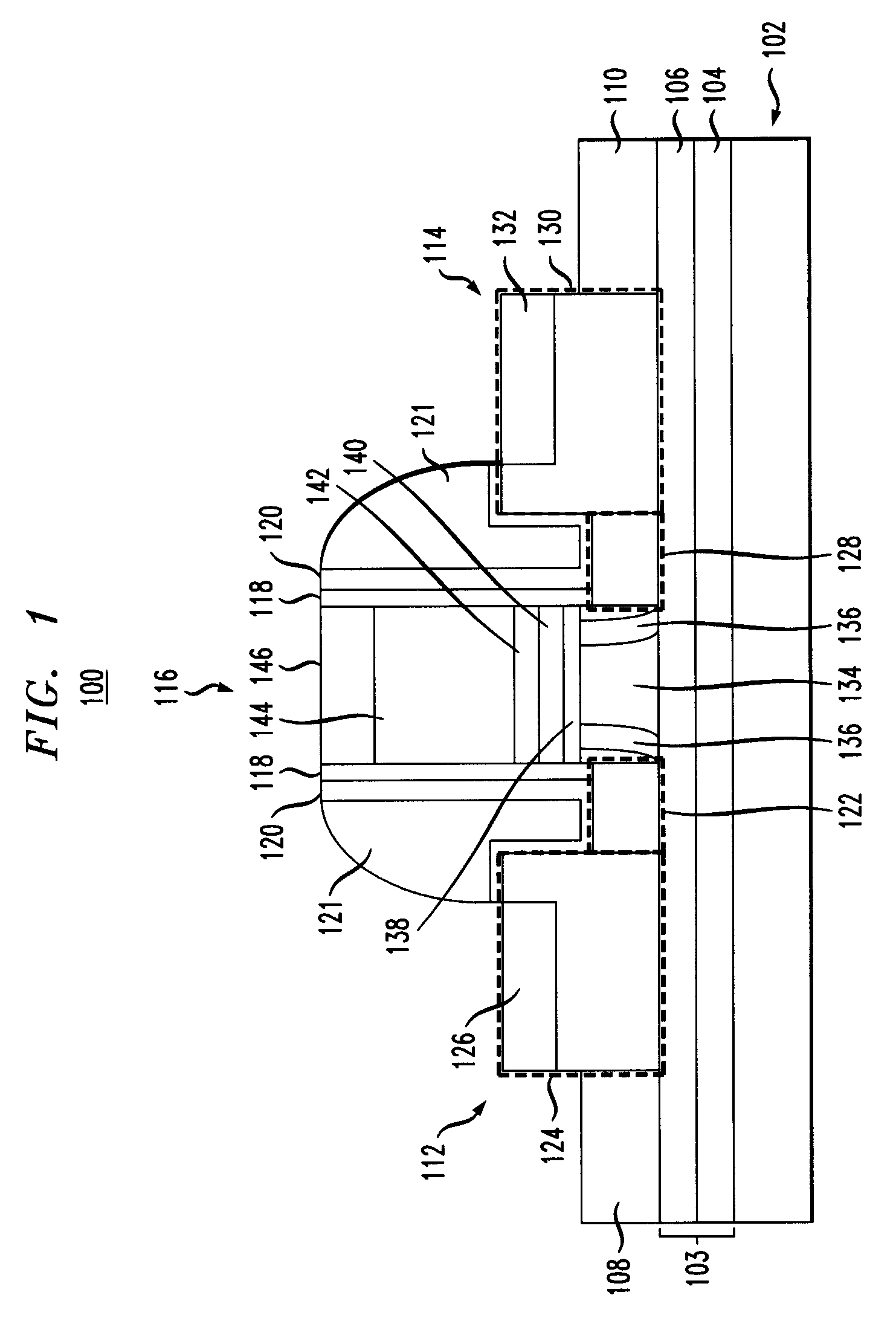
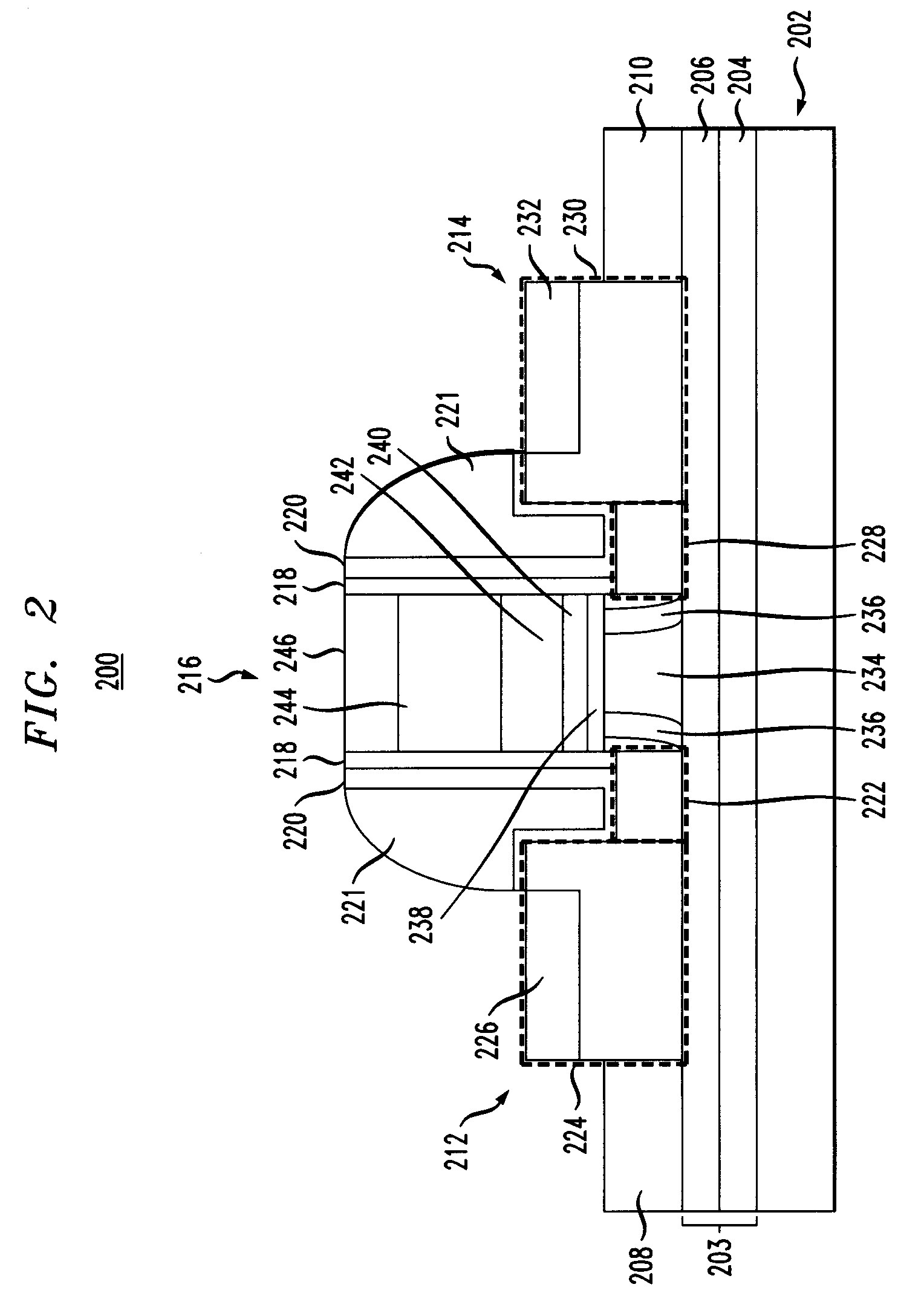
[0014]FIG. 1 is a cross-sectional diagram illustrating exemplary metal-oxide semiconductor field effect transistor (MOSFET) device 100. According to an exemplary embodiment, MOSFET device 100 is either an n-channel MOSFET (NMOSFET) (abbreviated hereinafter as “NFET”) device or a p-channel MOSFET (PMOSFET) (abbreviated hereinafter as “PFET”) device. MOSFET device 100 comprises substrate 102 having shallow trench isolation (STI) regions 108 / 110 and source / drain regions 112 / 114 formed therein, gate stack 116 separated from substrate 102 by interfacial oxide layer 138 and nitride spacers 118 / offset spacers 120 / source / drain diffusion spacers 121 adjacent to gate stack 116.

[0015]Substrate 102 comprises a silicon-on-insulator (SOI) substrate. As will be described in detail below, substrate 102 is formed from a thin SOI wafer, such as an ultra-thin SOI (UTSOI) wafer or an extra-thin SOI (ETSOI) wafer having a buried oxide (BOX) layer present between two semiconductor layers. According to an...


PUM


Abstract

Metal-oxide semiconductor field effect transistor (MOSFET) devices having metal gate stacks and techniques for improving performance thereof are provided. In one aspect, a metal-oxide semiconductor device is provided comprising a substrate having a buried oxide layer at least a portion of which is configured to serve as a primary background oxygen getterer of the device; and a gate stack separated from the substrate by an interfacial oxide layer. The gate stack comprises a high-K layer over the interfacial oxide layer; and a metal gate layer over the high-K layer.

Description

FIELD OF THE INVENTION[0001]The present invention relates to metal-oxide semiconductor field effect transistor (MOSFET) devices, and more particularly, to metal-gated MOSFET devices and techniques for scaling metal gate stack thickness so as to improve device performance.BACKGROUND OF THE INVENTION[0002]Metal-oxide semiconductor field effect transistor (MOSFET) devices are used in many integrated circuit designs, serving as switches to open and close the circuits. In general, a MOSFET device comprises a source region and a drain region connected by a channel, and a gate stack separated from the channel by a gate dielectric. The channel can comprise an n-type or p-type semiconductor material, forming an n-channel MOSFET (NMOSFET) or a p-channel MOSFET (PMOSFET) device, respectively.[0003]Traditionally, the gate stack in a MOSFET device would comprise a semiconductor material, such as silicon, over a nitride-containing layer, which serves as the gate dielectric. Current research, howe...

Claims


Application Information

Patent Timeline
IPC IPC(8): H01L29/786H01L21/336
CPCH01L29/4908H01L29/6653H01L29/66628H01L29/78621H01L29/78603H01L29/78606H01L29/66772
Inventor MAJUMDAR, AMLANMO, RENEE TONGREN, ZHIBINSLEIGHT, JEFFREY
Owner GLOBALFOUNDRIES INC
Why Eureka
Try Eureka