Perovskite oxide, ferroelectric film and ferroelectric device containing the perovskite oxide

a technology of perovskite oxide and ferroelectric film, which is applied in the field of perovskite oxide, ferroelectric film and ferroelectric device containing perovskite oxide, can solve the problems of deteriorating ferroelectric performance, difficult to reduce the thickness of bulk bodies below 20 micrometers, and the inability to use si substrates in piezoelectric devices manufactured by a process, etc., to suppress the deterioration of ferroelectric performance and enhance the enhancement of ferr

Inactive Publication Date: 2009-05-07
FUJIFILM CORP
View PDF9 Cites 17 Cited by
  • Summary
  • Abstract
  • Description
  • Claims
  • Application Information

AI Technical Summary

Benefits of technology

[0013]The first object of the present invention is to provide a PZT-based perovskite oxide which is doped with A-site substitute ions in the concentration exceeding 1 mol % and B-site substitute ions in the concentration of 10 mol % or more, is superior in ferroelectric performance such as piezoelectric performance, and can be produced without A-site defect.
[0014]The second object of the present invention is to provide a PZT-based ferroelectric film which is composed of a PZT-based ferroelectric oxide doped with A-site substitute ions in the concentration exceeding 1 mol % and B-site substitute ions in the concentration of 10 mol % or more, is superior in ferroelectric performance such as piezoelectric performance, and can be formed on a Si substrate without use of a sintering assistant.
[0037]The perovskite oxide according to the first aspect of the present invention is a PZT-based perovskite oxide which can be produced by doping with A-site substitute ions in the concentration exceeding 1 mol % and B-site substitute ions in the concentration of 10 mol % or more without doping with a sintering assistant. Specifically, the perovskite oxide according to the first aspect of the present invention is doped with A-site donor ions in the high concentration exceeding 1 mol % up to 40 mol % and B-site donor ions in the high concentration of 10 mol % to 40 mol %. Therefore, the perovskite oxide according to the first aspect of the present invention exhibits superior ferroelectric performance (piezoelectric performance). Since the perovskite oxide according to the first aspect of the present invention can be doped with high-concentration donor ions in both of the A-sites and the B-sites without doping with a sintering assistant, it is possible to suppress the deterioration of the ferroelectric performance which is caused by the doping with the sintering assistant, and thus maximize the enhancement of the ferroelectric performance realized by the doping with the donor ions.
[0038]In the perovskite oxide according to the first aspect of the present invention, the substitute ions at the A sites can reduce the A-site loss by making up for the Pb loss (which is likely to occur, for example, during sintering of PZT). Therefore, according to the present invention, it is possible to suppress the deterioration of the ferroelectric performance.
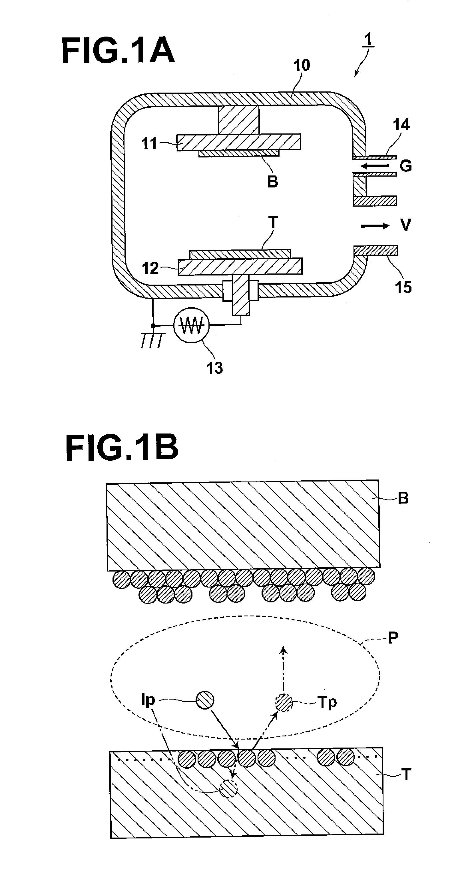
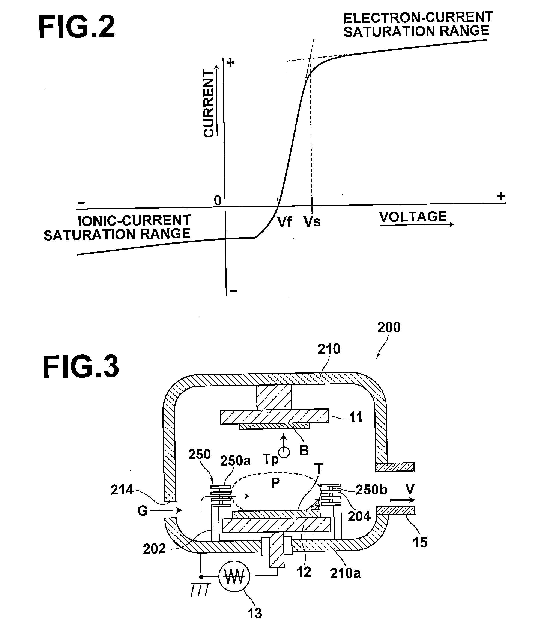
[0039]Further, since the ferroelectric film according to the second aspect of the present invention can be formed, for example, by a non-thermal equilibrium process, the ferroelectric film according to the second aspect of the present invention can be formed below the temperature at which reaction between Si and Pb can occur. Thus, according to the present invention, it is possible to form a ferroelectric film containing a PZT-based perovskite oxide on a Si substrate without doping with a sintering assistant, where the PZT-based perovskite oxide is doped with A-site donor ions in the high concentration exceeding 1 mol % up to 40 mol % and B-site donor ions in the high concentration of 10 mol % to 40 mol %, and exhibits superior ferroelectric performance.

Problems solved by technology

However, it is difficult to reduce the thickness of the bulk bodies below 20 micrometers.
Although it is preferable that the substrates used in the piezoelectric devices be Si substrates since Si substrates have satisfactory workability, the Si substrates cannot be used in the piezoelectric devices manufactured by a process which includes baking at the temperature of 800° C. or higher because reaction between the Si substrates and Pb in PZT can occur when the Si substrates are heated to the temperature of 800° C. or higher.
However, when the Si substrate is used, the ferroelectric performance deteriorates, so that it is difficult to sufficiently obtain the effect of the doping with the donor ions.
In addition, since Pb in the PZT-based ferroelectric films is likely to sublime, Pb loss (defect) is likely to occur.
There is a tendency for the ferroelectric performance to deteriorate when loss in the A-site atoms occurs.
However, it is known that the sol-gel technique is likely to produce Pb loss.

Method used


Image

  • Perovskite oxide, ferroelectric film and ferroelectric device containing the perovskite oxide
  • Perovskite oxide, ferroelectric film and ferroelectric device containing the perovskite oxide
  • Perovskite oxide, ferroelectric film and ferroelectric device containing the perovskite oxide

Examples


examples 1

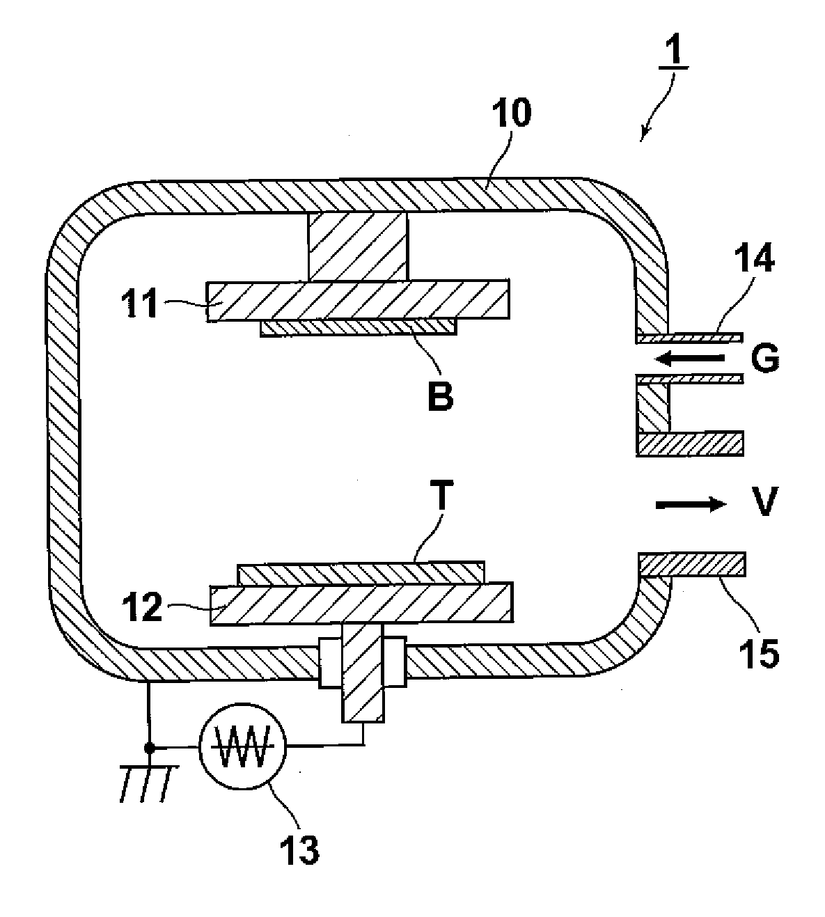
8.1 CONCRETE EXAMPLES 1

[0188]A plurality of ferroelectric films as the concrete examples 1 according to the present invention have been produced as follows.

[0189]First, substrates having an electrode have been produced by forming by sputtering Ban adhesion layer of titanium (Ti) having a thickness of 10 nm and a lower electrode of iridium (Ir) having a thickness of 150 nm in this order on a SOI (silicon-on-insulator) substrate with a diameter of 6 inches.

[0190]Next, four different types of Bi- and Nb-codoped PZT ferroelectric films (which are hereinafter referred to as Bi,Nb-PZT films) have been formed on the above substrates in the atmosphere of a mixture of Ar and 1.0 volume percent O2 at the degree of vacuum of 0.5 Pa by using different targets having different compositions, respectively. The four different types of Bi,Nb-PZT films are PZT-based ferroelectric films respectively doped with different amounts of niobium (Bi) at the A sites. The film-formation temperature is 525° C.,...

examples 2

8.5 CONCRETE EXAMPLES 2

[0206]A La- and Nb-codoped PZT ferroelectric film (La, Nb-PZT film), a Nd- and Nb-codoped PZT ferroelectric film (Nd, Nb-PZT film), a Ba- and Nb-codoped PZT ferroelectric film (Ba,Nb-PZT film), and a Sr- and Nb-codoped PZT ferroelectric film (Sr,Nb-PZT film) in which the molar fraction of the A-site element La, Nd, Ba, or Sr is 4% (x=0.04) have been produced as the concrete examples 2 according to the present invention in a similar manner to the concrete examples 1 except that the above ferroelectric films as the concrete examples 2 are respectively doped with La, Nd, Ba, and Sr, instead of Bi. In addition, piezoelectric devices and inkjet recording heads containing the above ferroelectric films have been produced in a similar manner to the concrete examples 1.

[0207]Further, the piezoelectric constants of the the above four ferroelectric films as the concrete examples 2 formed in the inkjet recording heads have been measured in a similar manner to the concrete...


PUM

PropertyMeasurementUnit
ionic radiusaaaaaaaaaa
thicknessaaaaaaaaaa
thicknessaaaaaaaaaa

Abstract

A perovskite oxide having a composition expressed by a compositional formula,(Pb1-x+δAx)(ZryTi1-y)1-zMzOw,where Pb and A are A-site elements, Zr, Ti, and M are B-site elements, A represents one or more A-site elements other than Pb, M represents one or more of elements Nb, Ta, V, Sb, Mo, and W, x, y, and z satisfy inequalities,0.01<x≦0.4,0<y≦0.7, and0.1≦z≦0.4, andδ is approximately 0, w is approximately 3, δ and w may deviate from 0 and 3, respectively, within ranges of δ and w in which the composition expressed by the compositional formula (Pb1-x+δAx)(ZryTi1-y)1-z-MzOw can substantially realize a perovskite structure.

Description

BACKGROUND OF THE INVENTION[0001]1. Field of the Invention[0002]The present invention relates to a perovskite oxide, a ferroelectric film containing the perovskite oxide, and a ferroelectric device and a liquid discharge device using the ferroelectric film.[0003]2. Description of the Related Art[0004]Currently, the piezoelectric devices each of which are constituted by a piezoelectric body and electrodes are used, for example, as piezoelectric actuators installed in inkjet recording heads. In order to realize high-speed highly-fine printing by use of an inkjet recording head, it is necessary to increase the density at which the piezoelectric devices are arranged. Therefore, techniques for reducing the thicknesses of the piezoelectric devices are currently being studied. From the viewpoint of the precision in machining or processing, it is preferable that the piezoelectric body in a piezoelectric device used in such an inkjet recording head have a form of a thin film.[0005]In additio...

Claims


Application Information

Patent Timeline
Patent Type & Authority Applications(United States)
IPC IPC(8): C04B35/035B32B19/00B41J2/045B41J2/055B41J2/135B41J2/14B41J2/16C01G25/02C01G33/00H01L21/316H01L41/09H01L41/18H01L41/187H01L41/316H01L41/39
CPCC04B35/491H01L41/316C04B2235/3241C04B2235/3251C04B2235/3258C04B2235/3272C04B2235/3275C04B2235/3279C04B2235/3286C04B2235/3289C04B2235/3298C23C14/088H01L41/0805H01L41/1876C04B2235/3227H10N30/1051H10N30/8554H10N30/076
Inventor ARAKAWA, TAKAMI
Owner FUJIFILM CORP
Why Eureka
Try Eureka