

Electronic device and method for producing electronic device
- Summary
- Abstract
- Description
- Claims
- Application Information
AI Technical Summary
Benefits of technology
Problems solved by technology
Method used
Image

Examples
examples
[0045]The invention is described in more detail with reference to the following Examples, in which the material used, its amount and the ratio, the details of the treatment and the treatment process may be suitably modified or changed not deviating the gist and the scope of the invention. Accordingly, the invention should not be limitatively interpreted by the Examples mentioned below.
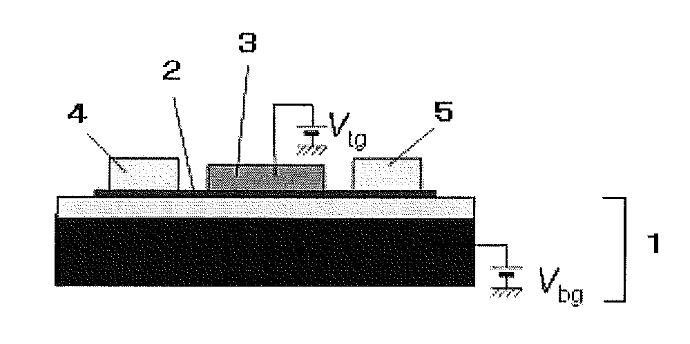
[0046]An electronic device having the constitution of FIG. 1 was produced. Concretely, it was produced according to the following process.
[0047]Highly-oriented pyrolytic graphite (HOPG) (NT-MDT's GRBS) was cleaved on an adhesive tape, and pressed to a Si substrate with 300 nm-thick oxidized layer on the surface (Ferrotec Silicone's 12488-131A), whereby the kish graphite was adhered to the substrate. Using an optical microscope observation, an electron beam resist was applied thereto, and this was processed through electron beam lithography and metal vapor deposition (titanium, 50 nm thick), and a sourc...
PUM
| Property | Measurement | Unit |
|---|---|---|
| Thickness | aaaaa | aaaaa |
| Thickness | aaaaa | aaaaa |
| Thickness | aaaaa | aaaaa |
Abstract
Description
Claims
Application Information