
Method of making an applicator liquid for electronics fabrication process

Active Publication Date: 2009-06-04
ZEON CORP
View PDF98 Cites 16 Cited by
  • Summary
  • Abstract
  • Description
  • Claims
  • Application Information

AI Technical Summary

Benefits of technology

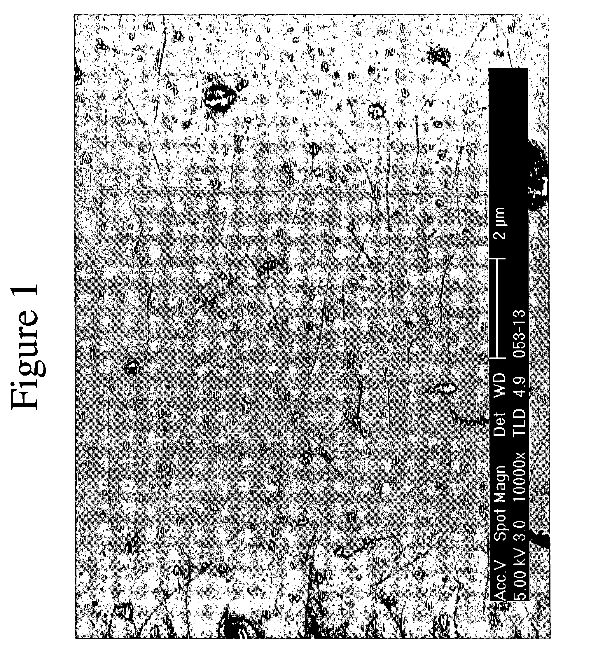
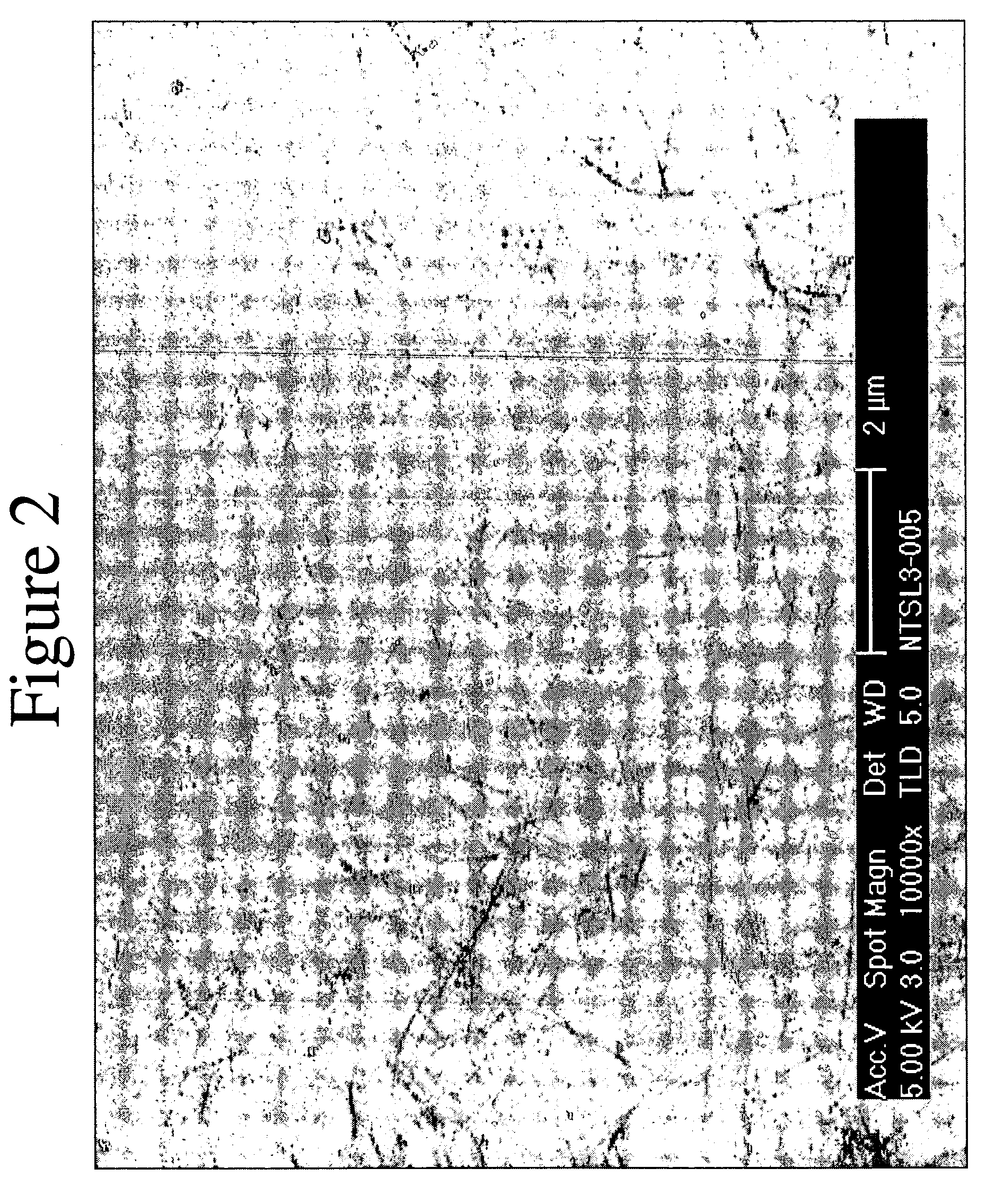
[0017]According to one aspect of the present invention, nanotube films having high standards of non-toxicity and purity are provided. Such films may be fabricated in semiconductor fabrication processes, for example, CMOS and advanced logic and memory fabrications. Such fabrication processes may produce devices having fine features, e.g., ≦250 nm.

Problems solved by technology

However, the inclusion or incorporation of the SWNT as part of standard microelectronic fabrication process has faced challenges due to a lack of a readily available application method compatible with existing semiconductor equipment and tools and meeting the stringent materials standards required in the electronic fabrication process.
Individual nanotubes may be used as conducting elements, e.g. as a channel in a transistor, however the placement of millions of catalyst particles and the growth of millions of properly aligned nanotubes of specific length presents serious challenges.
Nanotubes may be derivatized in order to facilitate bringing the tubes into solution, however in uses where pristine nanotubes are necessary, it is often difficult to remove the derivatizing agent.
Even when removal of the derivatizing agent is not difficult, such removal is an added, time-consuming step.
Polymer wrapping usually affects sheet resistance of the SWNT network and may not be appropriate for electronic applications where low sheet resistance is desired.
While these approaches were successful in solubilizing the SWNTs in a variety of organic solvents to practically relevant levels, all such attempts resulted in the depletion of the π electrons that are essential to retain interesting electrical and optical properties of nanotubes.
While this type of approach has helped to retain the electrical conductivity and optical properties of the SWNTs, most such methods leave halogens or alkali metals or polymeric residues, which tend to severely hamper any meaningful use in microelectronic fabrication facilities.

Method used


Image

  • Method of making an applicator liquid for electronics fabrication process
  • Method of making an applicator liquid for electronics fabrication process

Examples


example 1

[0056]This example describes the purification of nanotubes.

[0057]Single-walled carbon nanotubes (SWNTs) were purified by stirring in 7.7M HNO3 for 8 h followed by refluxing at 125° C. for 12 h. The acid refluxed material was washed with DI water three times by a sonication-centrifugation-decantation cycle. The DI water washed material was then vacuum filtered over a 5 micron filter until a dried SWNT membrane was obtained on the filter paper. This purified SWNT material was collected and used for making a SWNT composition.

example 2

[0058]This example describes the preparation of a nanotube composition and a nanotube article.

[0059]In order to avoid recontamination of the nanotubes, clean room conditions, for example, Class 100 or greater, were maintained during preparation and processing of the nanotube composition. Twenty-one mg of single-walled nanotubes (SWNTs), purified as described above in Example 1 were soaked in 10 mL ethyl lactate (electronics grade—Sigma), ground with a mortar and pestle, sonicated and centrifuged to remove the supernatant. These steps were repeated as necessary to solubilize the carbon nanotubes. The solubilized nanotubes had a final concentration of 21 mg carbon nanotubes per 250 mL ethyl lactate, and the optical density at 550 nm of the solution was measured to be 1.001.

[0060]Each individual step of the solubilization process is detailed in the Table 1 for the solubilization of SWNTs in ethyl lactate (EL). This protocol is illustrative of one means of forming a solubilized nanotube...

example 3

[0061]This example describes an alternative method of preparing a nanotube composition.

[0062]Twenty-one mg carbon nanotubes were mixed in 10 mL EL and subjected to sonication, centrifugation, decanting of the supernatant and remixing of carbon nanotubes in EL for repeated sonication until the tubes were sufficiently solubilized; i.e., the nanotubes were subjected essentially the same steps as in Example 2, without grinding with mortar and pestle. The steps of the process are shown in Table 2.

TABLE 2Alternate Process Flow Chart for SWNT solubilization in Ethyl-LactateStepProcessDurationRemarks1Place 100 mg in 800 ml ELN / AIn 1 L polypropylene (PP) bottle.2Add Teflon impellersN / AIn 1 L PP bottle3Place on autoshaker100hPowered through a timer4Collect in a 1 L RBN / AHF cleaned flask, in cleanroom5Bath sonicate1h5° C.6Centrifuge (15 krpm, 15° C.)2h6 × 250; Beckman PP bottles7Decant supernatant~15minCollect in 1000 ml flask8Check for optical density at 550N / AIf above 1.25 this needs to be a...


PUM


Abstract

Certain spin-coatable liquids and application techniques are described, which can be used to form nanotube films or fabrics of controlled properties. A method of making an applicator liquid containing nanotubes for use in an electronics fabrication process includes characterizing an electronic fabrication process according to fabrication compatible solvents and allowable levels of metallic and particle impurities; providing nanotubes that satisfy the allowable impurities criteria for the electronics fabrication process; providing a solvent that meets the fabrication compatible solvents and allowable impurities criteria for the electronic fabrication process; and dispersing the nanotubes into the solvent at a concentration of at least one milligram of nanotubes per liter solvent to form an applicator liquid.

Description

CROSS-REFERENCE TO RELATED APPLICATIONS[0001]This application is related to the following applications, all of which are assigned to the assignee of this application, and all of which are incorporated by reference in their entirety: Nanotube Films and Articles (U.S. Pat. No. 6,706,402) filed Apr. 23, 2002; Methods of Nanotube Films and Articles (U.S. patent application Ser. No. 10 / 128,117) filed Apr. 23, 2002; and Patterning of Nanoscopic Articles (U.S. Provisional Patent Appl. No. 60 / 501,033) filed on Sep. 8, 2003.BACKGROUND[0002]1. Technical Field[0003]This invention describes spin-coatable liquids for use in the preparation of nanotube films. Such liquids are used in creating films and fabrics of nanotubes or mixtures of nanotubes and other materials on a variety of substrates including silicon, plastics, paper and other materials. In particular, the invention describes spin-coatable liquids containing nanotubes for use in electronics fabrication processes. Furthermore, the spin-...

Claims


Application Information

Patent Timeline
IPC IPC(8): H01B1/04
CPCB82Y10/00B82Y30/00B82Y40/00H01L51/0048C01B31/026C01B2202/02H01L51/0007C01B31/0253Y10S977/847Y10S977/845C01B32/168C01B32/17H10K71/15H10K85/221
Inventor SEN, RAHULSIVARAJAN, RAMESHRUECKES, THOMASSEGAL, BRENT M.
Owner ZEON CORP
Learn More