Method of Film Deposition and Film Deposition System

a film deposition and film technology, applied in the field of film deposition and film deposition systems, can solve the problems of difficult to find out some materials having such a low work function and strict design rules, and achieve the effect of lowering the threshold value of the gate electrode and low work function

Inactive Publication Date: 2009-06-04
TOKYO ELECTRON LTD
View PDF7 Cites 1 Cited by
  • Summary
  • Abstract
  • Description
  • Claims
  • Application Information

AI Technical Summary

Benefits of technology

[0010]In view of the aforementioned problems in the prior art and in order to solve them effectively, we accomplished the present invention. Accordingly, an object of the present invention is to provide a method of film deposition and a film decomposition system that can deposit a thin film of a metallic compound of a high-melting-point metal, whose carbon density is sufficiently enhanced so that the thin film can achieve low work function, resulting in lowering of a threshold value of a gate electrode.
[0011]The inventors have earnestly studied a method of film deposition for depositing a thin film of a metallic compound of a high-melting-point metal. As a result, the inventors have found out that, in the case of CVD (Chemical Vapor Deposition), when a partial pressure of an ammonium gas is set lower than a predetermined value, carbon density in the film is sufficiently raised, so that work function and the threshold value of a gate electrode can be reduced.
[0012]In addition, the inventors have found out that, when a material gas and an ammonium gas or the like are alternatively and repeatedly supplied into the processing vessel, carbon density in the film can be sufficiently raised.

Problems solved by technology

Recently, design rules have become very strict.
However, as a material of an nMOS gate electrode, it is still difficult to find out some materials having such a low work function as 4.1 eV.

Method used


Image

  • Method of Film Deposition and Film Deposition System
  • Method of Film Deposition and Film Deposition System
  • Method of Film Deposition and Film Deposition System

Examples


first embodiment

[0072]The first embodiment of the method of film deposition according to the present invention will be described.

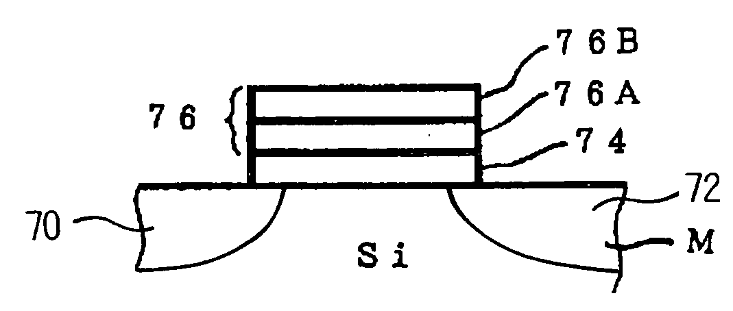
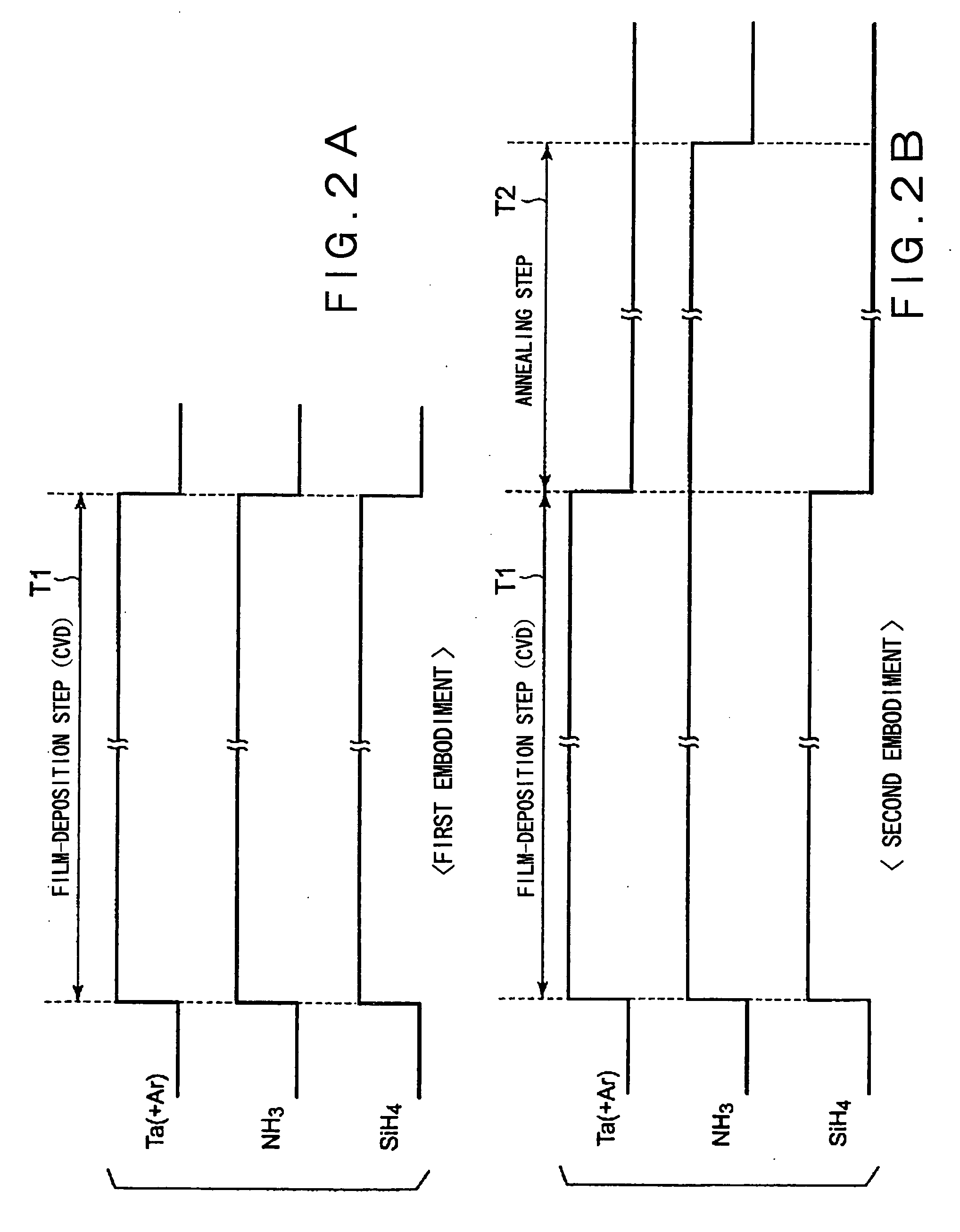
[0073]FIG. 2A is a diagram showing a gas supply mode in the first embodiment of the method of the invention. FIG. 9A shows the major film-deposition conditions and the analysis result of the formed thin film. As described above, herein, as a thin film of a metallic compound, a silicon tantalum nitride film containing carbon (TaSiN containing C) is formed.

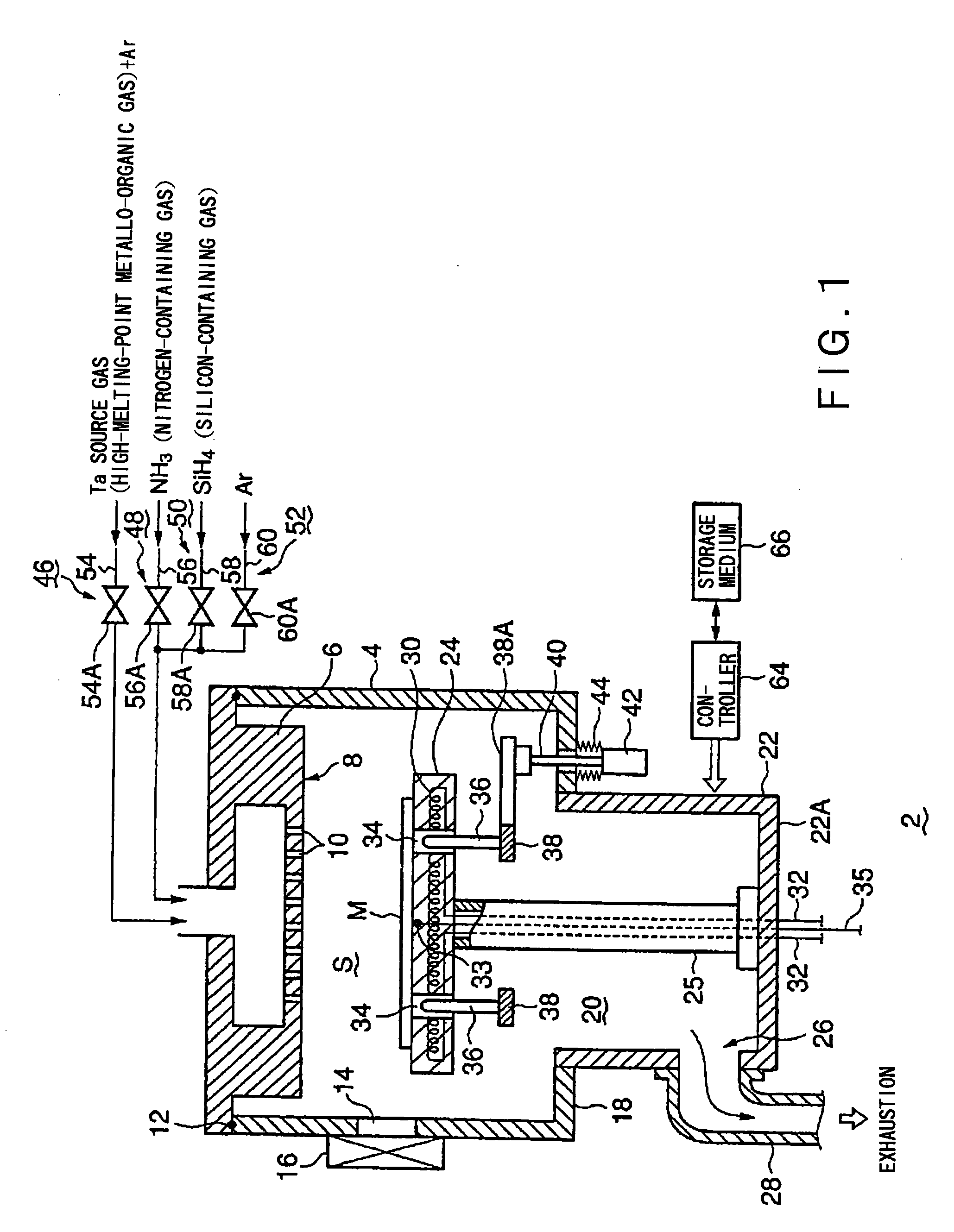
[0074]As shown in FIG. 2A, a Ta source gas (herein, Taimato), an NH3 gas and a monosilane gas (SiH4) are simultaneously supplied into the processing vessel 4, and a film-deposition process is conducted by a CVD process for a predetermined time (film-deposition time) T1.

[0075]Thus, a TaSiN film containing C is formed. The process conditions are explained as follows. The process temperature is preferably within a range of 300 to 700° C., for example being set at 600° C. The process pressure is preferably within a range of 5...

second embodiment

[0077]The second embodiment of the method of film deposition according to the present invention will be described.

[0078]FIG. 2B is a diagram showing a gas supply mode in the second embodiment of the method of the invention. FIG. 9A shows the major film-deposition conditions and the analysis result of the formed thin film.

[0079]As shown in FIG. 2B, in the second embodiment, an annealing process is conducted to the thin film, which has been formed according to the first embodiment, under an in-situ situation without exposing the wafer M to the atmospheric air. For example, after the film-deposition process, the annealing process (annealing step) is conducted in the same processing vessel 4 without taking out the wafer M from the processing vessel 4. More concretely, after the completion of the film-deposition step, the supply of the Ta source gas and of the SiH4 gas is stopped, but the supply of the NH3 gas is continued, so that the annealing process is conducted for a predetermined t...

third embodiment

[0089]The third embodiment of the method of film deposition according to the present invention will be described.

[0090]FIG. 4A is a diagram showing a gas supply mode in the third embodiment of the method of the invention. FIG. 9A shows the major film-deposition conditions and the analysis result of the formed thin film.

[0091]In the first embodiment and the second embodiment, during the film-deposition process, the NH3 gas and the SiH4 gas are supplied. However, in the third embodiment, the supply of the both gases is stopped, and only the Ta source gas is supplied. That is, as shown in FIG. 4A, the Ta source gas is supplied together with the Ar carrier gas, and a thin film is deposited for a predetermined time T3 by means of a CVD process. The thin film doesn't contain Si, but organic components of the Ta source gas are dissociated, so that a TaN film containing C is formed as the thin film (see the third embodiment in FIG. 9A).

[0092]The process conditions are explained as follows. ...


PUM

PropertyMeasurementUnit
Work Functionaaaaaaaaaa
work functionaaaaaaaaaa

Abstract

The present invention is a method of film deposition that comprises a film-depositing step of supplying a high-melting-point organometallic material gas and a nitrogen-containing gas to a processing vessel that can be evacuated, so as to deposit a thin film of a metallic compound of a high-melting-point metal on a surface of an object to be processed placed in the processing vessel. A partial pressure of the nitrogen-containing gas during the film-depositing step is 17% or lower, in order to increase carbon density contained in the thin film.

Description

BACKGROUND OF THE INVENTION[0001]1. Field of the Invention[0002]The present invention relates to a method of film deposition for forming a thin film on an object to be processed, such as a semiconductor wafer, and to a film deposition system.[0003]2. Background Art[0004]Generally, in the production of semiconductor integrated circuits, objects to be processed, such as semiconductor wafers, are repeatedly subjected, sheet by sheet, to various processing steps, such as film deposition, etching, heat treatment, modification, and recrystallization, thereby obtaining desired integrated circuits. Moreover, the recent demand for thinner integrated circuits having higher levels of integration has made the line width, film thickness, etc. of integrated circuits much smaller than ever.[0005]Metallic compound films of high-melting-point organometallic materials tend to be often used as materials that show relatively low resistivity even when they are made thinner than ever and patterned to hav...

Claims


Application Information

Patent Timeline
Patent Type & Authority Applications(United States)
IPC IPC(8): H01L29/78C23C16/54H01L21/768
CPCC23C16/34C23C16/45523C23C16/56H01L29/518H01L21/28556H01L29/517H01L21/28194
Inventor YAMASAKI, HIDEAKIKAWANO, YUMIKO
Owner TOKYO ELECTRON LTD
Why Eureka
Try Eureka