Transistor with A-Face Conductive Channel and Trench Protecting Well Region

a technology of transistor and conductive channel, applied in the direction of basic electric elements, electrical apparatus, semiconductor devices, etc., can solve the problems of marginal improvement in achieving the desired increase, the development of the mosfet on the a-face, and the inability to achieve optimal performance in the power mosfet context, and achieve the effect of high voltage blocking ability

Active Publication Date: 2009-06-11
WOLFSPEED INC
View PDF18 Cites 50 Cited by
  • Summary
  • Abstract
  • Description
  • Claims
  • Application Information

AI Technical Summary

Benefits of technology

[0016]The invention is a new transistor structure (50) that optimizes current along the A-face of a silicon carbide body (65) while minimizing the JFET effect in the drift region (55) during forward con

Problems solved by technology

Yano's design, however, is not preferable in vertical power devices because the Yano devices have a lower critical field and conduct under reversed bias at lower gate voltages than desired.
The sole technique of developing the MOSFET on the a-face, without additional parameters being adjusted as well, has not proven to be the best answer in the context of optimizing performance in power MOSFETs.
Although research efforts have studied these approaches extensively, DMOSFETs (double diffused metal oxide semiconductors FETs) and UMOSFETs (trench gated metal oxide semiconductor FETs) of the prior art have shown only marginal improvements in achieving the desired increase in channel mobility.
For example, known UMOSFETs show an increased carrier density in the conductive channel, but these same devices suffer from the electrical field crowding at the trench gate corners under reverse bias.
Ion implantation is difficult to achieve accurately in DMOSFETs, and the resulting devices are limited in channel mobility.
The problem with the prior art UMOSFET is that the corner of the trench (42) exhibits a noted crowding of the electric field at the corner of the trench, inhibiting current flow through the drift region (43) and the substrate (44) down to the drain (32).
The field crowding also results in a lower sustaine

Method used


Image

  • Transistor with A-Face Conductive Channel and Trench Protecting Well Region
  • Transistor with A-Face Conductive Channel and Trench Protecting Well Region
  • Transistor with A-Face Conductive Channel and Trench Protecting Well Region

Examples


Embodiment Construction

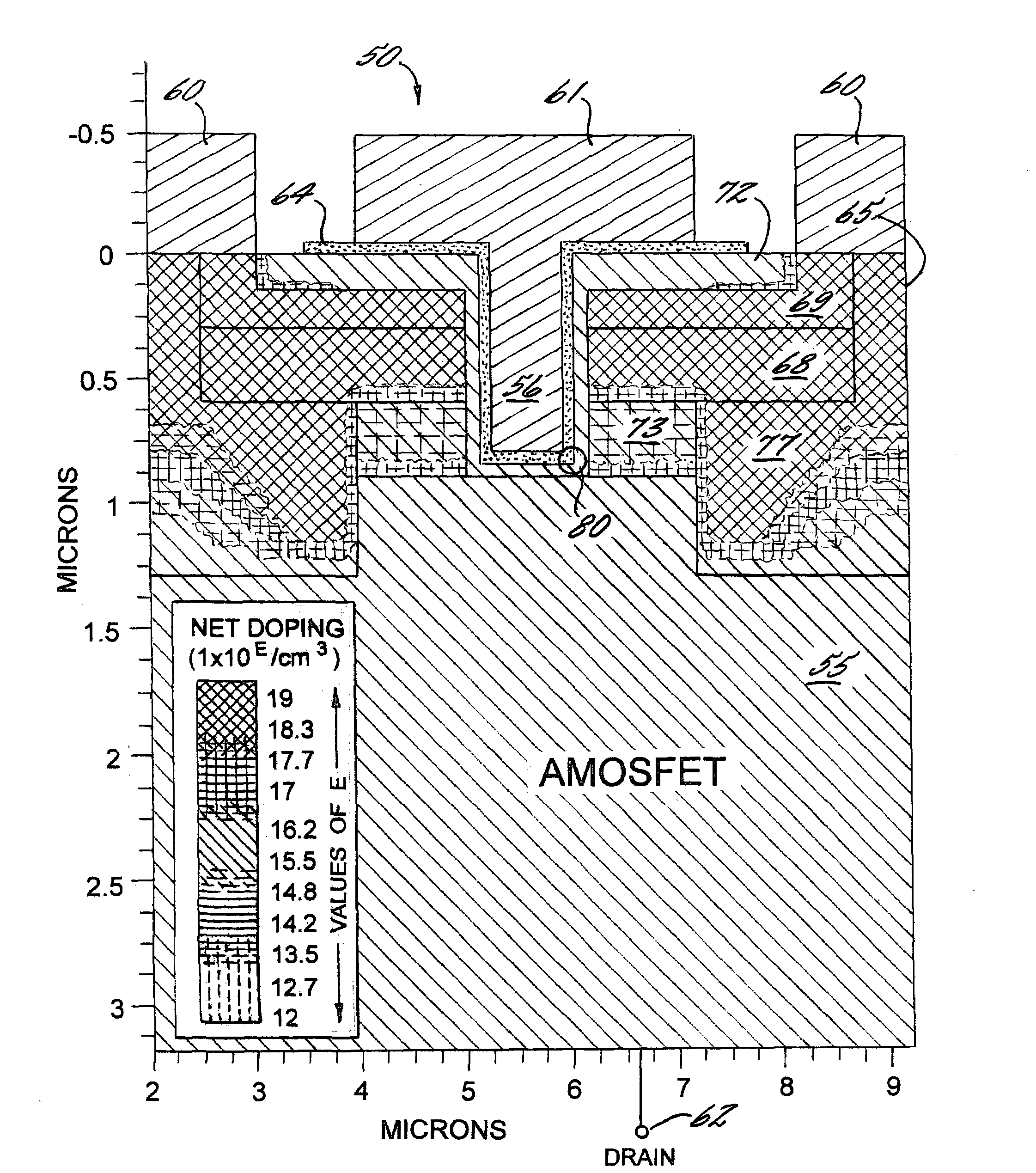
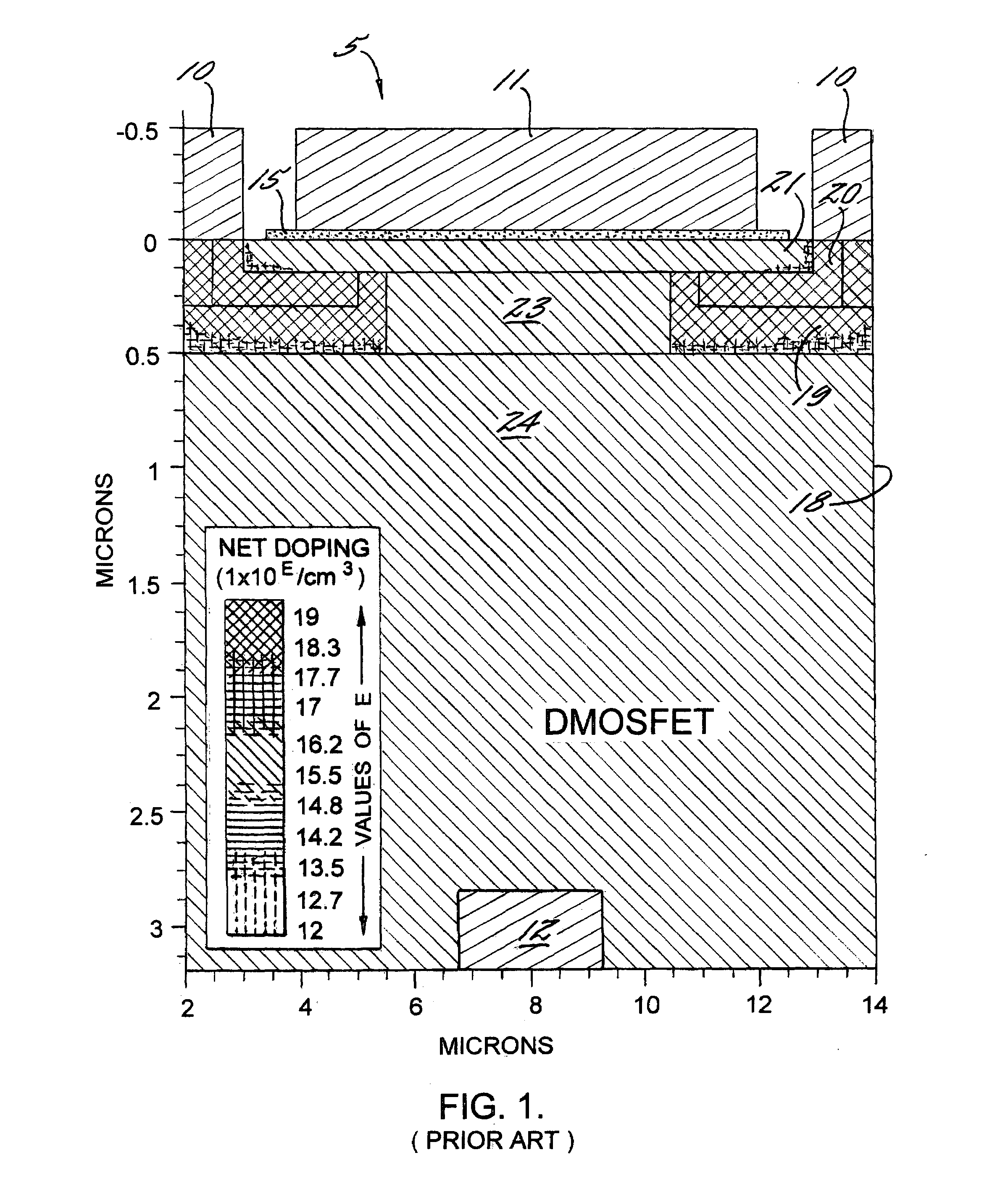
[0035]The MOSFET of this invention includes a conductive channel on the A-face of a silicon carbide crystal epitaxial layer for increased channel mobility (e.g., up to 200 cm2 / Vs for the AMOSFET vs. 100 cm2 / Vs or less for prior art DMOSFETs). FIG. 5 sets forth the structure of the new AMOSFET (50). The drift region (55), or current spreading layer, supports epitaxial layers forming the active region of the AMOSFET (50) with current flowing from a source region (60) through the drift region (55), to the drain (62). Broadly, the AMOSFET (50) is a transistor having an insulated gate (61), or control contact, within a trench (56) in a semiconductor crystal structure (58). The trench (56) defines a pair of semiconductor mesas (65) that each encompass a p+ type layer (68) and an n+ type layer (69) forming a pn junction therein. The p+ type layer (68) is an epitaxial layer positioned under a buried channel (72) and between the trench (56) and a p+ doped well (77). The n+ type layer (69) is...


PUM


Abstract

A transistor structure optimizes current along the A-face of a silicon carbide body to form an AMOSFET that minimizes the JFET effect in the drift region during forward conduction in the on-state. The AMOSFET further shows high voltage blocking ability due to the addition of a highly doped well region that protects the gate corner region in a trench-gated device. The AMOSFET uses the A-face conduction along a trench sidewall in addition to a buried channel layer extending across portions of the semiconductor mesas defining the trench. A doped well extends from at least one of the mesas to a depth within the current spreading layer that is greater than the depth of the trench. A current spreading layer extends between the semiconductor mesas beneath the bottom of the trench to reduce junction resistance in the on-state. A buffer layer between the trench and the deep well further provides protection from field crowding at the trench corner.

Description

BACKGROUND[0001]The invention relates to transistor structures, particularly useful in MOSFETs, in which the conductive channel is formed on the A-face of the semiconductor body. The problems addressed by this invention include (i) reducing channel resistance in the on-state for optimal current output and (ii) minimizing field crowding effects to maximize the reverse voltage blocking capabilities within the device.[0002]Over the last twenty years, transistor designs have been optimized to achieve a controlled current flow in the on-state while simultaneously having the ability to block certain voltages in the off-state. The development of better semiconductor materials, including silicon carbide and the Group III nitrides, has led to extraordinary advancements in transistor design that allow greater control over transistor performance in both the on-state (e.g., higher current output) and the off-state (higher voltage blocking with less leakage current). Silicon carbide has been of ...

Claims


Application Information

Patent Timeline
IPC IPC(8): H01L29/24H01L29/78H01L29/74H01L21/04
CPCH01L29/045H01L29/0615H01L29/0847H01L29/0878H01L29/7828H01L29/1608H01L29/749H01L29/7813H01L29/1095
Inventor ZHANG, QINGCHUNAGARWAL, ANANTJONAS, CHARLOTTE
Owner WOLFSPEED INC
Why Eureka
Try Eureka