Semiconductor device and manufacturing method therefor

a semiconductor device and capacitor technology, applied in semiconductor devices, capacitors, electrical devices, etc., can solve the problems of columnar lower electrodes, b, fall down, etc., and achieve the effect of reliable semiconductor devices, improved mechanical support strength of plate-like supports, and large capacitan

Active Publication Date: 2009-06-11
LONGITUDE SEMICON S A R L
View PDF5 Cites 11 Cited by
  • Summary
  • Abstract
  • Description
  • Claims
  • Application Information

AI Technical Summary

Benefits of technology

[0046]According to a method of manufacturing a semiconductor device of the present invention, in the formation of the through-hole which penetrates the second nitride film as the plate-like support, the through-hole is aligned so that the length of the part where the through-hole is overlapped with the pore portion is shorter than the length of the part where the through-hole is not overlapped with the pore portion in the planar view. Therefore, it can be ensured that the length of the contacting portion where the cylindrical lower electrode formed on the through-hole is contacted with the second nitride film is half or more than half of the circumference length of the cylindrical lower electrode, and the cylindrical lower electrode is not separated from the second nitride film which becomes the plate-like support. Thus, when the second oxide film and the first oxide film are removed, the cylindrical lower electrode can be completely prevented from falling down, and a reliable semiconductor device can be manufactured. Also, in the semiconductor device of t...

Problems solved by technology

However, in the case of forming a capacitor by using the above constitution and increasing the superficial area, there are problems that the columnar-shaped lower electrode 512 may lack physical stability because a high aspect ratio is needed, and thus the columnar lower electrode 512 may fall down in the middle of the manufacturing process.
Furthermore, in the case of increasing the superficial area by making the lower electrode 512 in a tubular shape, it is necessary to thin the film thickness of the tubular-shaped columnar portion 512a, therefore the columnar lower electrode 512 may lack physical stability, and may fall down in the middle of the manufacturing process.
When a capacitor is formed in such a state, an electrical short circuit may be caused, therefore it is a big problem as a semiconductor device.
Therefore, in a layout shown in FIGS. 11A and 11B in which the lower electrodes are aligned densel...

Method used


Image

  • Semiconductor device and manufacturing method therefor
  • Semiconductor device and manufacturing method therefor
  • Semiconductor device and manufacturing method therefor

Examples


embodiment 1

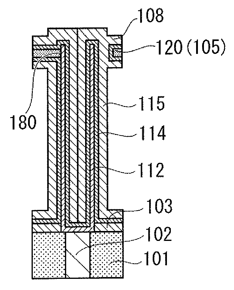
[0067]FIGS. 6A to 6C are drawings which show an example of a memory array of DRAM, which is an embodiment of the present invention. FIG. 6A is a schematic plan view of a lower electrode in a memory array region. FIGS. 6B and 6C are schematic cross-sectional views taken along the line A to A′ in FIG. 6A.

[0068]As shown in FIG. 6A, the lower electrode 112 is in a circular shape in the planar view, and a plurality of lower electrodes are densely aligned in a memory array region. Here, the term “densely aligned” represents a condition in which the lower electrodes are aligned most efficiently and in the high density in order not to cause useless space in the planar space of a memory array. Therefore, the lower electrode is in a circular shape in the planar view, and even when any lower electrode is selected, six lower electrodes are aligned around the single lower electrode. Also, the distance between the center of each lower electrode is approximately equal mutually. Also, it is clear t...

embodiment 2

[0080]Next, another embodiment of a semiconductor device of the present invention will be described below.

[0081]A capacitor is formed in the same manner as the embodiment 1, except that a pore portion 171, which differs in the shape and the size from the pore portion 170b, is formed instead of the pore portion 170b described in the embodiment 1. Hereinafter, common members in the embodiments 1 and 2 will be described using the same numbers and letters.

[0082]FIG. 7 shows a planar view wherein a plurality of ellipsoidal pore portions 171 are formed in the plate-like support 120. The total area of the plurality of pore portions 171 is shorter than the total area of the plate-like support 120 where the pore portions 171 are not formed. Through the pore portions 171, a first oxide film 104 formed at the lower layer can be seen.

[0083]FIG. 8 is a schematic planar view showing a plurality of cylindrical lower electrodes 112 formed in the plate-like support 120 in which an ellipsoidal pore p...

embodiment 3

[0087]Next, another embodiment of a semiconductor device of the present invention will be described below.

[0088]A capacitor is formed in the same manner as in the embodiment 1, except that a pore portion 172, which differs in the shape and the size from the pore portion 170, is formed instead of the pore portion 170 described in the embodiment 1. Hereinafter, common members of the embodiments 1 and 3 will be described using the same numbers and letters.

[0089]FIG. 9 shows a planar view in which a plurality of ellipsoidal pore portions are formed in a plate-like support 120. The ellipsoidal pore portion 172 of the embodiment 3 differs from the ellipsoidal pore portion 171 of the embodiment 2 in the point that the ellipsoidal pore portion 172 has a longer major axis than the ellipsoidal pore portion 171. The total area of the plurality of pore portions 172 is shorter than the total area of the plate-like support 120 where the pore portions 172 are not formed. Through the pore portions ...


PUM


Abstract

This semiconductor device according to the present invention includes a plurality of cylindrical lower electrodes aligned densely in a memory array region; a plate-like support which is contacted on the side surface of the cylindrical lower electrodes, and links to support the plurality of the cylindrical lower electrodes; a pore portion provided in the plate-like support; a dielectric film covering the entire surface of the cylindrical lower electrodes and the plate-like support in which the pore portion is formed; and an upper electrode formed on the surface of the dielectric film, wherein the boundary length of the part on the side surface of the cylindrical lower electrode which is exposed on the pore portion is shorter than the boundary length of the part on the side surface of the cylindrical lower electrode which is not exposed on the pore portion.

Description

BACKGROUND OF THE INVENTION[0001]1. Field of the Invention[0002]The present invention relates to a semiconductor device with a capacitor, particularly a semiconductor device with a cylindrical type of a capacitor, and a manufacturing method thereof.[0003]Priority is claimed on Japanese Patent Application No. 2007-126538, filed on May 11, 2007, the content of which is incorporated herein by reference.[0004]2. Description of Related Art[0005]Generally, a cell of dynamic random access memory (hereinafter, referred to as DRAM) is composed of a transistor and a capacitor. The capacitor is composed of a lower electrode (first electrode), a dielectric film and an upper electrode (second electrode). As the size of the DRAM gets smaller, the space occupied by the cell also becomes smaller. In order to acquire a certain amount of capacitance in the limited occupied-space, it is required to make an electrode structure of the capacitor to be three-dimensional, thereby increasing a superficial a...

Claims


Application Information

Patent Timeline
IPC IPC(8): H01L27/108H01L21/44
CPCH01L27/0207H01L27/10817H01L28/60H01L28/91H01L27/10852H10B12/318H10B12/033
Inventor HIROTA, TOSHIYUKI
Owner LONGITUDE SEMICON S A R L
Why Eureka
Try Eureka