Semiconductor device and manufacturing method thereof
a technology of semiconductor devices and manufacturing methods, applied in semiconductor devices, semiconductor/solid-state device details, electrical apparatus, etc., can solve the problems of increasing the need to markedly reduce the annealing time in comparison with the conventional case, thermal stress variation of the threshold voltage of a circuit or crystal defect due to thermal stress, and time delay
- Summary
- Abstract
- Description
- Claims
- Application Information
AI Technical Summary
Benefits of technology
Problems solved by technology
Method used
Image

Examples
first embodiment
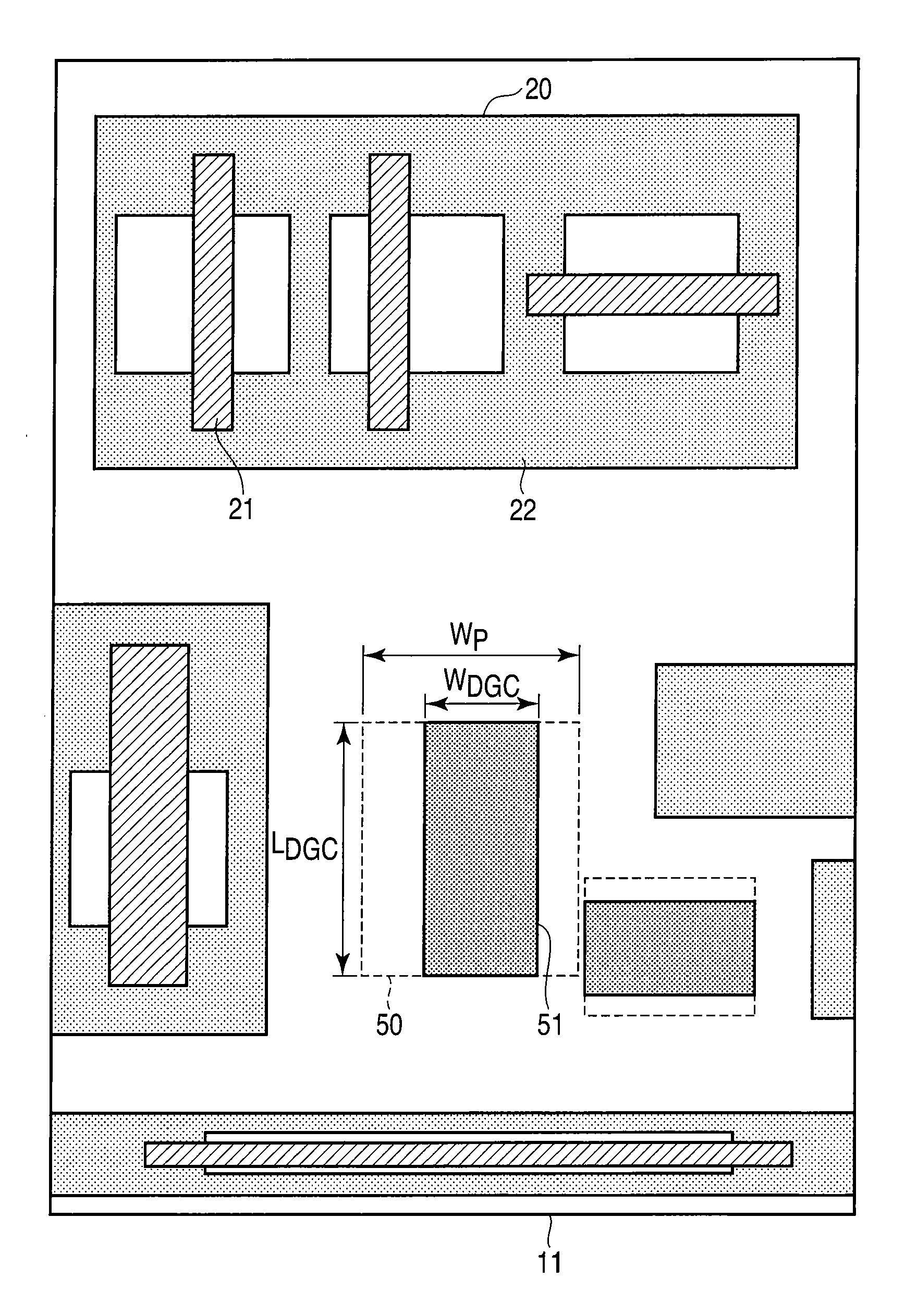
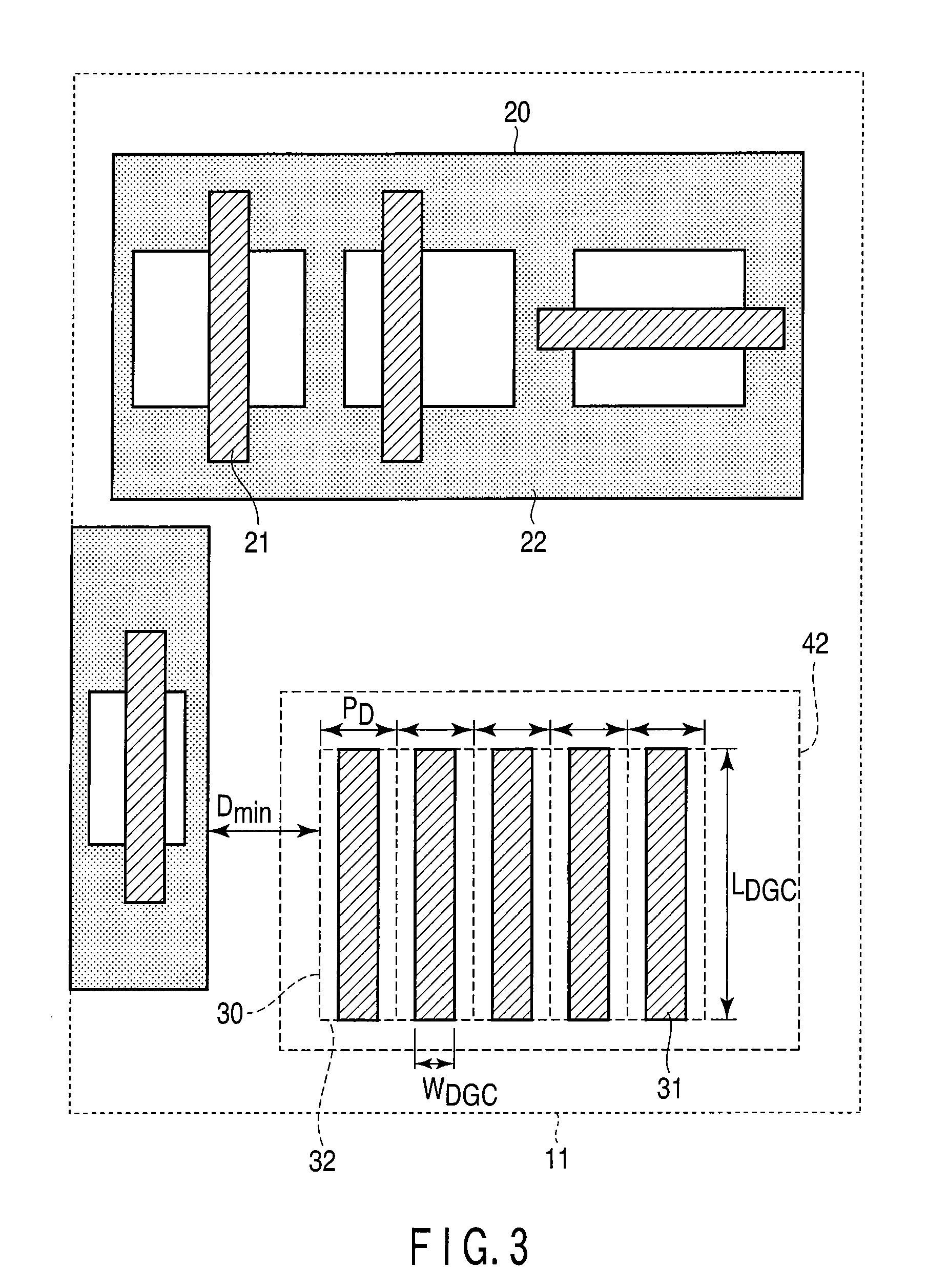
[0048]As shown in FIG. 3, a circuit pattern region 20 having integrated circuit patterns related to the circuit operation and a dummy pattern region 30 having dummy patterns that are not related to the circuit operation are arranged on a main surface 11 of a semiconductor substrate of Si or the like. The main surface 11 of the semiconductor substrate is subjected to an optical annealing process by means of a method called spike rapid thermal annealing (spike-RTA) in the semiconductor manufacturing process. The principal wavelength of irradiating light of spike-RTA is 1 μm. If the principal wavelength of irradiating light is greater than or equal to 1.5 μm, the light passes through the semiconductor substrate and heat cannot be generated in the semiconductor substrate. Therefore, it is necessary to set the principal wavelength less than or equal to 1.5 μm.
[0049]The circuit pattern region 20 is configured by GCs (gate patterns) 21 and STI region (element isolation pattern) 22.
[0050]Th...
second embodiment
[0074]In the first embodiment, the dummy pattern region configured by the dummy GCs is described, but in the present embodiment, a dummy pattern region configured by a dummy STI region is considered. As shown in FIG. 11, a semiconductor integrated circuit configured by a circuit pattern region 20 and dummy pattern region 70 is arranged on a semiconductor substrate main surface 11. In FIG. 11, portions that are the same as those of FIG. 3 are denoted by the same symbols and the detailed explanation thereof is omitted.
[0075]The circuit pattern region 20 is configured by GCs 21 and STI region 22. In this case, it is supposed that the circuit pattern region 20 has a feature in a region smaller than the principal wavelength and the light absorption rate in the circuit pattern region 20 is set to 80% to 85%. Further, the dummy pattern region 70 in which dummy STI regions (dummy element isolation patterns) 71 are repeatedly arranged is provided in a coarse region.
[0076]The number of repeti...
third embodiment
[0088]As shown in FIG. 16, a semiconductor integrated circuit region 100 is formed on a semiconductor substrate main surface 11 as a partial region of the whole portion of a semiconductor integrated circuit. The semiconductor integrated circuit region 100 is divided into square regions 110 having one side whose length is equal to the thermal diffusion length. In each of the square regions 110, a dummy pattern group 112 that is a set of dummy patterns is arranged. It is supposed that each of the dummy patterns of the dummy pattern group 112 is the same as the dummy pattern descried in the first or second embodiment. A fine circuit pattern region 111 is a region in which a fine circuit pattern having a feature in a region smaller than the principal wavelength is arranged. In this case, in each of the square regions 110, the dummy patterns are arranged so that the total value of the coverage factors of the fine circuit pattern region 111 and the region occupied by the dummy pattern gro...
PUM
 Abstract
Description
Claims
Application Information
 - R&D
- Intellectual Property
- Life Sciences
- Materials
- Tech Scout
- Unparalleled Data Quality
- Higher Quality Content
- 60% Fewer Hallucinations
Browse by: Latest US Patents, China's latest patents, Technical Efficacy Thesaurus, Application Domain, Technology Topic, Popular Technical Reports.
© 2025 PatSnap. All rights reserved.Legal|Privacy policy|Modern Slavery Act Transparency Statement|Sitemap|About US| Contact US: help@patsnap.com