Fabricating methods of photoelectric devices and package structures thereof

Inactive Publication Date: 2009-06-18
ADVANCED OPTOELECTRONICS TECH
View PDF11 Cites 29 Cited by
  • Summary
  • Abstract
  • Description
  • Claims
  • Application Information

AI Technical Summary

Benefits of technology

[0011]An aspect of the present invention is to provide fabricating methods of photoelectric devices and package structures thereof. A ceramic substrate is adhered to a photoelectric semiconductor

Problems solved by technology

The package of a photoelectric product will seriously affect the photoelectric transformation efficiency of the die.
Because the limitation of the precision of a lead frame, the scale of the device cannot be unlimitedly miniaturized, and the reflection surface is difficultly formed.
There is a problem that resin materials cannot stand a high temperature when they are used to cover the lead frame.
In addition, due to the resin material cannot dissipate heat well, the increasing of the temperature of the photoelectric die causes a decrease in the light emitting efficiency.
The structure cannot bear the high tempera

Method used


Image

  • Fabricating methods of photoelectric devices and package structures thereof
  • Fabricating methods of photoelectric devices and package structures thereof
  • Fabricating methods of photoelectric devices and package structures thereof

Examples


Embodiment Construction

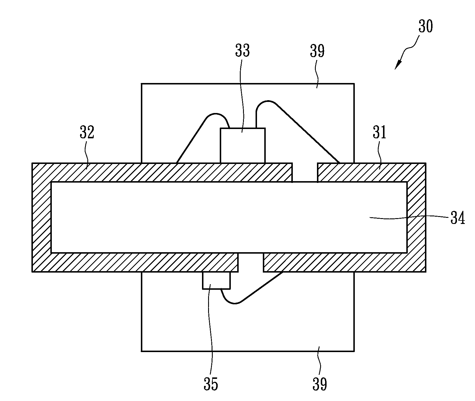
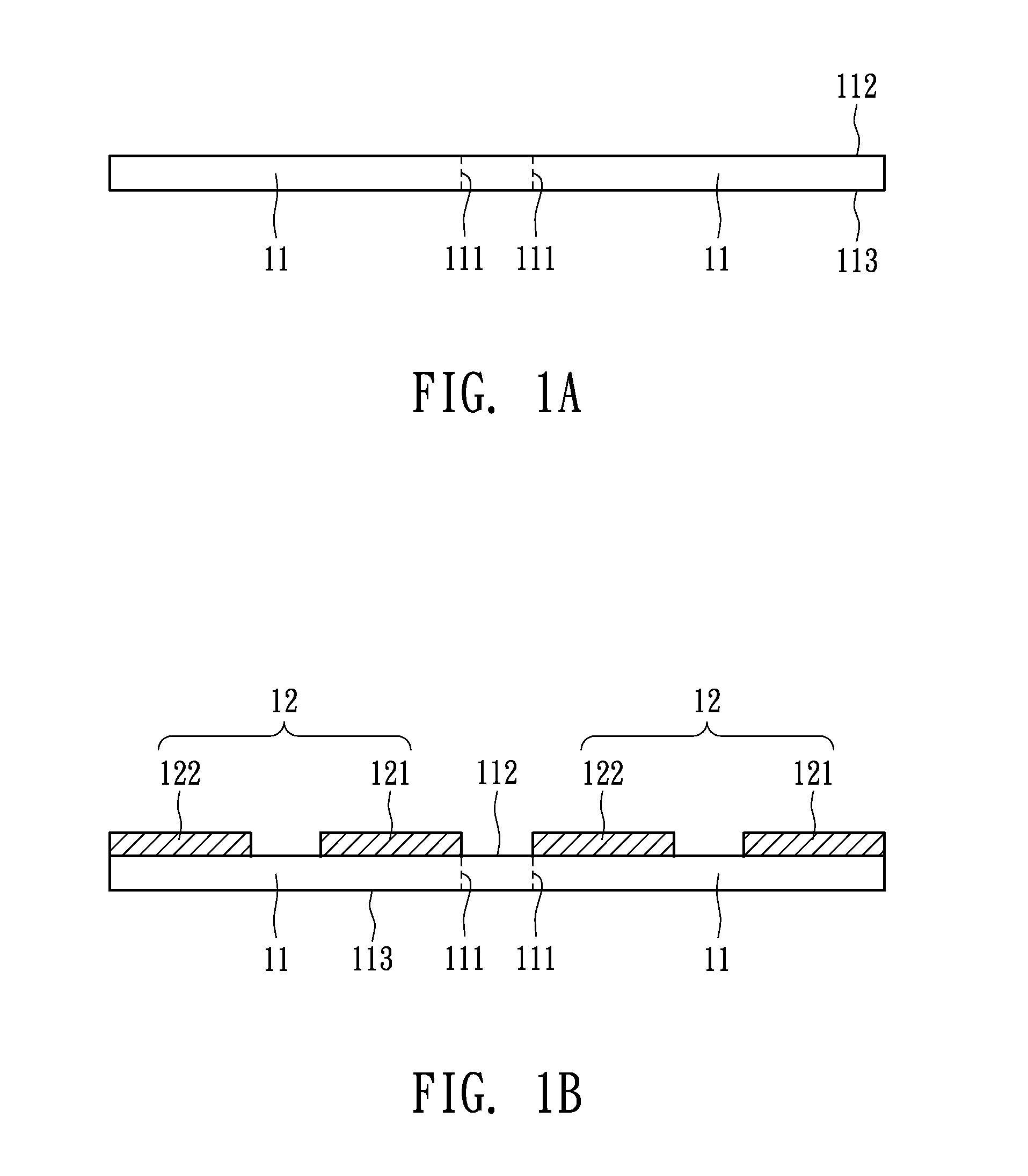
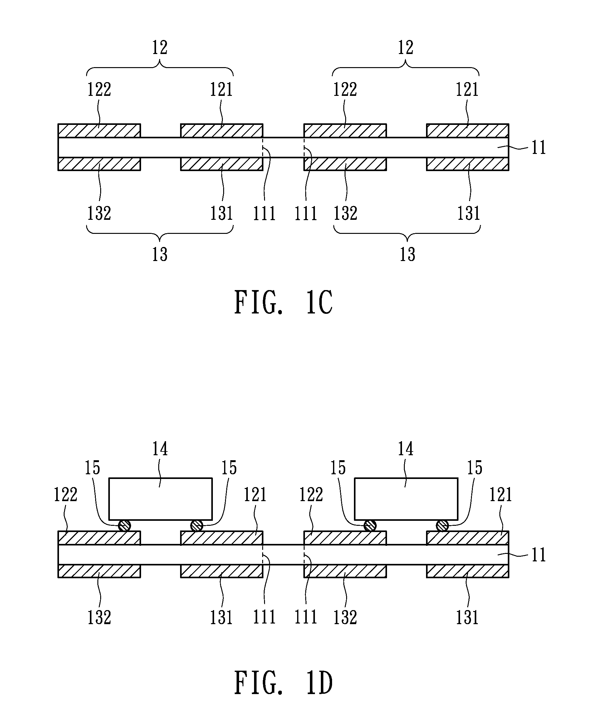
[0035]FIGS. 1A-1G are the diagrams illustrating the steps of the fabricating method of a photoelectric device in accordance with present invention. The cutting lines on the ceramic substrate 11 are formed with a LASER or a mold pressing. The most use material of the ceramic substrate is AlO. The other substitute materials comprise AlN, BeO, SiC, glass, Al, or diamond. The slurry preparation or slip preparation is the first step for making the ceramic substrate 11. The slurry is the combination of organic materials and inorganic materials, wherein a constant ratio of ceramic powder to glass powder are mixed for the inorganic materials, and organic materials comprise polymer binder, plasticizer and organic solvent, etc. The purposes of adding the glass powder into the inorganic material include adjustments of the thermal expansion character parameter of the ceramic substrate 11, adjustments of the character of a dielectric constant, and adjustments of a sintering temperature.

[0036]As ...


PUM


Abstract

The invention discloses a method for fabricating a photoelectric device. A ceramic substrate is first provided, and then a first patterned electrode and a second patterned electrode are formed on and underneath the surface of the ceramic substrate. A plurality of photoelectric devices is sequentially connected to the first electrode layer with a wire solder or a eutectic joint method. The encapsulation materials cover the each photoelectric die to prevent damaged from the external force or environment. Cutting the ceramic substrate along the spaces between the photoelectric dies forms a plurality of independent package units.

Description

BACKGROUND OF THE INVENTION[0001]1. Field of the Invention[0002]The present invention relates to fabricating methods of photoelectric devices and package structures thereof, and more particularly to methods and photoelectric devices using a die bonding process or a eutectic joint process to mount a photoelectric die.[0003]2. Description of the Related Art[0004]LEDs (light emitting diode) have advantages including small size, high illuminating efficiency and long life. They are anticipated to be the best light source for the future. Because of the rapid development of LCDs (liquid crystal display) and the trend of full-sized screen displays, white light LEDs are applied not only to indication lamps and large size screens but also to consumer electronics products (e.g., cell phones and personal digital assistants).[0005]A package structure can be seen as the protector of a semiconductor die and an interface of signal transmission. It serves dies not only for mounting, sealing and prot...

Claims


Application Information

Patent Timeline
IPC IPC(8): H01L27/00H01L21/00
CPCH01L25/167H01L31/0203H01L2924/12041H01L2924/01322H01L2224/73204H01L24/97H01L2224/16225H01L2924/09701H01L2224/48091H01L2224/48227H01L2924/00014H01L2924/00H01L2924/12035H01L2924/14H01L2924/15787H01L2924/181H01L2924/00012
Inventor TSENG, WEN LIANGCHEN, LUNG HSIN
Owner ADVANCED OPTOELECTRONICS TECH
Why Eureka
Try Eureka