Low noise and low input capacitance differential mds lna

a low noise, differential amplifier technology, applied in differential amplifiers, amplifiers with semiconductor devices/discharge tubes, amplifier details, etc., can solve distortion problems, complex interactions between input signals (or multiple input signals) and particular non-linearities of amplifiers, etc., to reduce the noise contribution of sub-threshold region biased transistors to the overall circuit output, and reduce input capacitance of novel differential amplifiers

Active Publication Date: 2009-06-18
QUALCOMM INC
View PDF4 Cites 35 Cited by
  • Summary
  • Abstract
  • Description
  • Claims
  • Application Information

AI Technical Summary

Benefits of technology

[0024]Because the gates of the transistors used to generate the cancel signals (the third and fourth transistors) are not coupled to the differential input signal nodes of the LNA as in a conventional MDS LNA, the input capacitance of the novel differential MDS LNA is reduced. Noise introduced into the output of the novel differential MDS LNA d...

Problems solved by technology

The interactions between the input signal (or multiple input signals) and the particular non-linearities of the amplifier can be complex, and the type of distortion can also be complex and depends on many different characteristics of the amplifier and the input signal.
Accordingly, a substantial amount of the transmitted signals may leak back into the receiver and cause distortion problems.
Because the cross-modulation component is in the receive band, it typically cannot be separated from the desired signal by filtering.
Thermal noise is due to random motion of electrons and atoms within the resistive component of any impedance such as the resistive component of the semiconductor material of which transistors are made.
All amplifiers utilizing transistors therefore introduce noise.
This noise is naturally occurring and inherent in the amplifier.
The introduction of noise into the output of the LNA cannot be eliminated, but poor design can result in the LNA adding noise m...

Method used


Image

  • Low noise and low input capacitance differential mds lna
  • Low noise and low input capacitance differential mds lna
  • Low noise and low input capacitance differential mds lna

Examples


Embodiment Construction

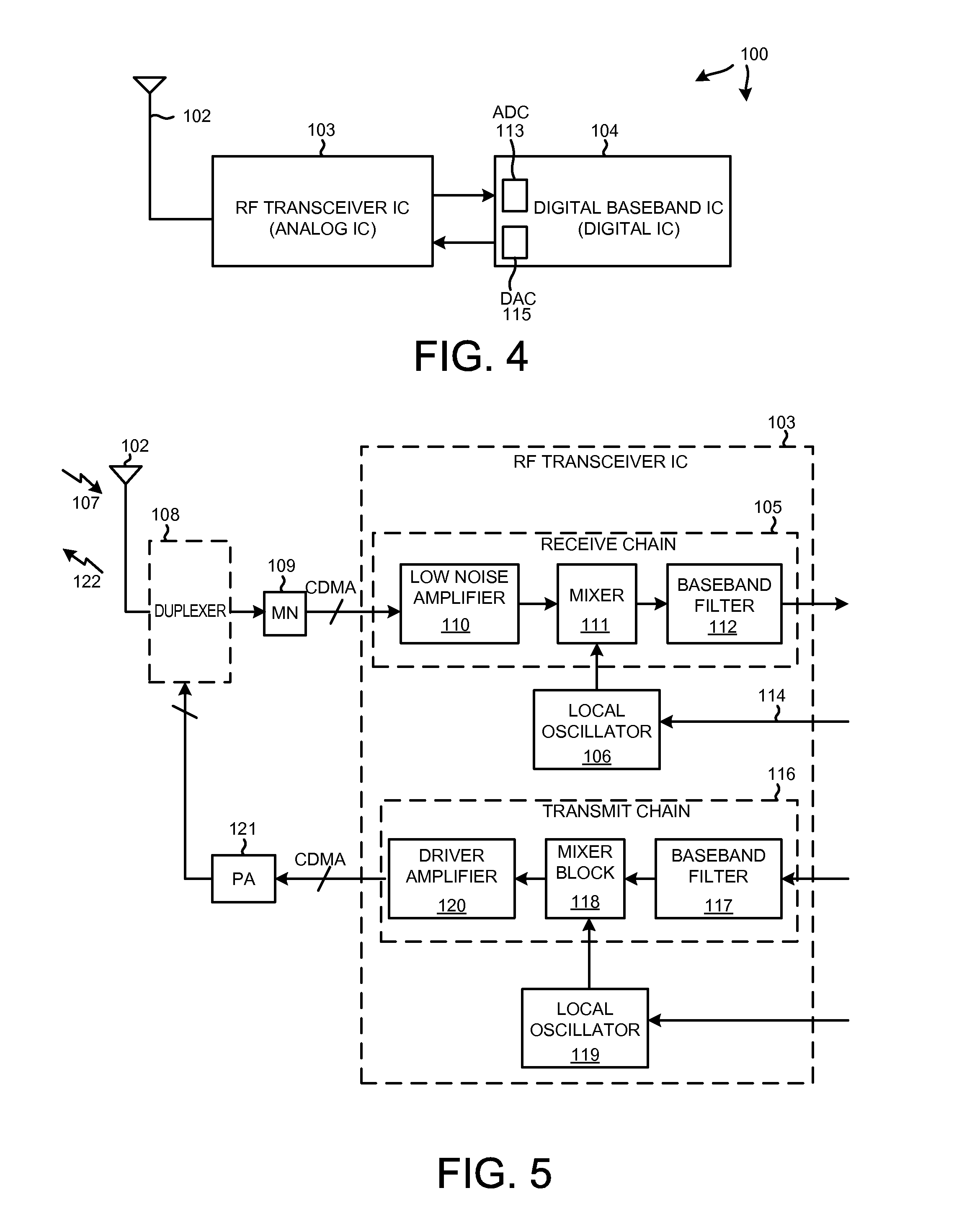
[0040]FIG. 4 is a very simplified high level block diagram of one particular type of mobile communication device 100 in accordance with one novel aspect. In this example, mobile communication device 100 is a 3-D cellular telephone that uses the CDMA2000 cellular telephone communication protocol. The cellular telephone includes (among several other parts not illustrated) an antenna 102 and two integrated circuits 103 and 104. Integrated circuit 104 is called a “digital baseband integrated circuit” or a “baseband processor integrated circuit”. Integrated circuit 103 is an RF transceiver integrated circuit. RF transceiver integrated circuit 103 is called a “transceiver” because it includes a transmitter as well as a receiver.

[0041]FIG. 5 is a more detailed block diagram of the RF transceiver integrated circuit 103 of FIG. 1. The receiver includes what is called a “receive chain”105 as well as a local oscillator (LO) 106. When the cellular telephone is receiving, a high frequency RF sig...


PUM


Abstract

A differential low noise amplifier (LNA) involves two main amplifying transistors biased in saturation, and two cancel transistors biased in sub-threshold. In one example, the gates of the cancel transistors are coupled to the drains of main transistors, in a symmetrical and cross-coupled fashion. The main transistors are source degenerated. Because the gates of cancel transistors are not coupled to the differential input leads of the LNA, the input capacitance of the LNA is reduced. Noise introduced into the LNA output due to the cancel transistors being biased in the sub-threshold region is reduced because there are two stages. The first stage involves the main transistors, and the second stage involves the cancel transistors. By increasing the gain of the first stage and decreasing the gain of the second stage, overall LNA gain is maintained while reducing the noise that the sub-threshold biased transistors contribute to the LNA output.

Description

BACKGROUND INFORMATION[0001]1. Technical Field[0002]The disclosed embodiments relate to low noise amplifiers.[0003]2. Background Information[0004]The first amplification stage in a radio receiver such as a receiver of a cellular telephone is generally an amplifier circuit called a Low Noise Amplifier (LNA). The LNA reduces the noise contributions of following stages and sets the lowest achievable noise level of the overall receiver. The LNA is therefore generally designed to have high gain to minimize the amount of noise introduced without introducing unacceptably large amounts of distortion. If a sinusoidal input signal of a pure single frequency is supplied to the input of a linear amplifier, then the amplifier will output an amplified version of the input signal. The output signal will have only a single frequency, and this frequency will be the frequency of the input signal. If, however, the same sinusoidal input signal is supplied to the input of an amplifier that exhibits an a...

Claims


Application Information

Patent Timeline
IPC IPC(8): H03F3/45
CPCH03F1/3205H03F1/3211H03F2203/45396H03F2203/45318H03F3/45188
Inventor CABANILLAS, JOSEGUDEM, PRASAD S.KIM, NAMSOOMARCU, CRISTIANSAVLA, ANUP
Owner QUALCOMM INC
Why Eureka
Try Eureka