Process for forming an organic electronic device including an organic device layer

a technology of electronic devices and organic materials, applied in the field of organic electronic devices, can solve the problems of difficult control of uniform formation and filling of many individual structures

Active Publication Date: 2009-06-18
LG CHEM LTD
View PDF21 Cites 11 Cited by
  • Summary
  • Abstract
  • Description
  • Claims
  • Application Information

AI Technical Summary

Problems solved by technology

However uniform formation and fill of many individual structures can be difficult to control.

Method used


Image

  • Process for forming an organic electronic device including an organic device layer
  • Process for forming an organic electronic device including an organic device layer
  • Process for forming an organic electronic device including an organic device layer

Examples


example 1

[0138]This examples illustrates the synthesis of bis-(3,3,4,4,5,5,6,6,7,7,8,8,8-tridecafluorooctyl)maleate (“PCSA-1”)

[0139]The 1H,1H,2H,2H-perfluoro-1-octanol (Aldrich) (36.2 grams, 99.4 mmole) was placed in a 250 ml flask under nitrogen and treated with maleic anhydride (4.06 grams, 41.4 mmole) followed by p-toluenesulfonic acid monohydrate (0.78 gram, 4.1 mmole). The mixture was stirred and heated under nitrogen to 113-115° C. to give a clear colorless liquid. The mixture was maintained at 113-115° C. for 65 minutes and then it was cooled to room temperature. The reaction mixture was chromatographed on a silica gel column (5 cm diameter and 19 cm long) using 15% ethyl acetate in hexane to give 27.07 grams (81%) of a colorless oil. The oil solidified after standing at room temperature. It was dissolved in a minimum amount (several milliliters) of ethyl acetate. The solution was diluted with approximately 40 ml of hexane to near cloud point. The solution was cooled in an ice bath an...

example 2

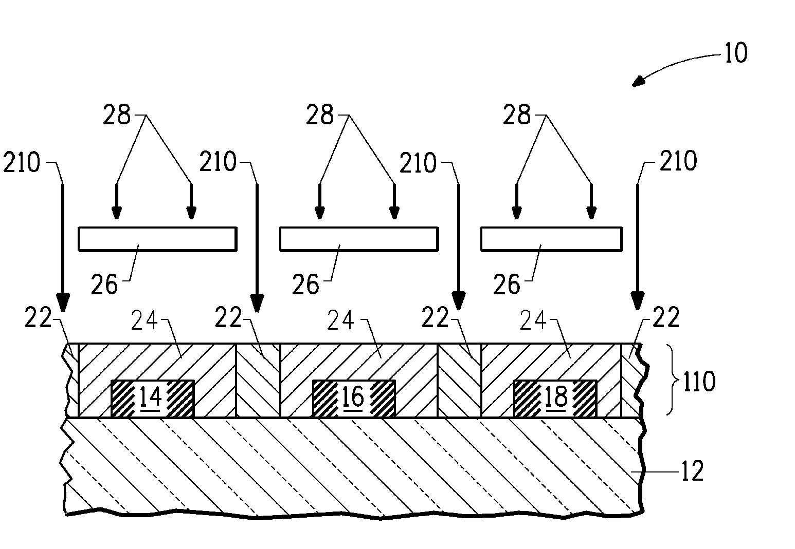
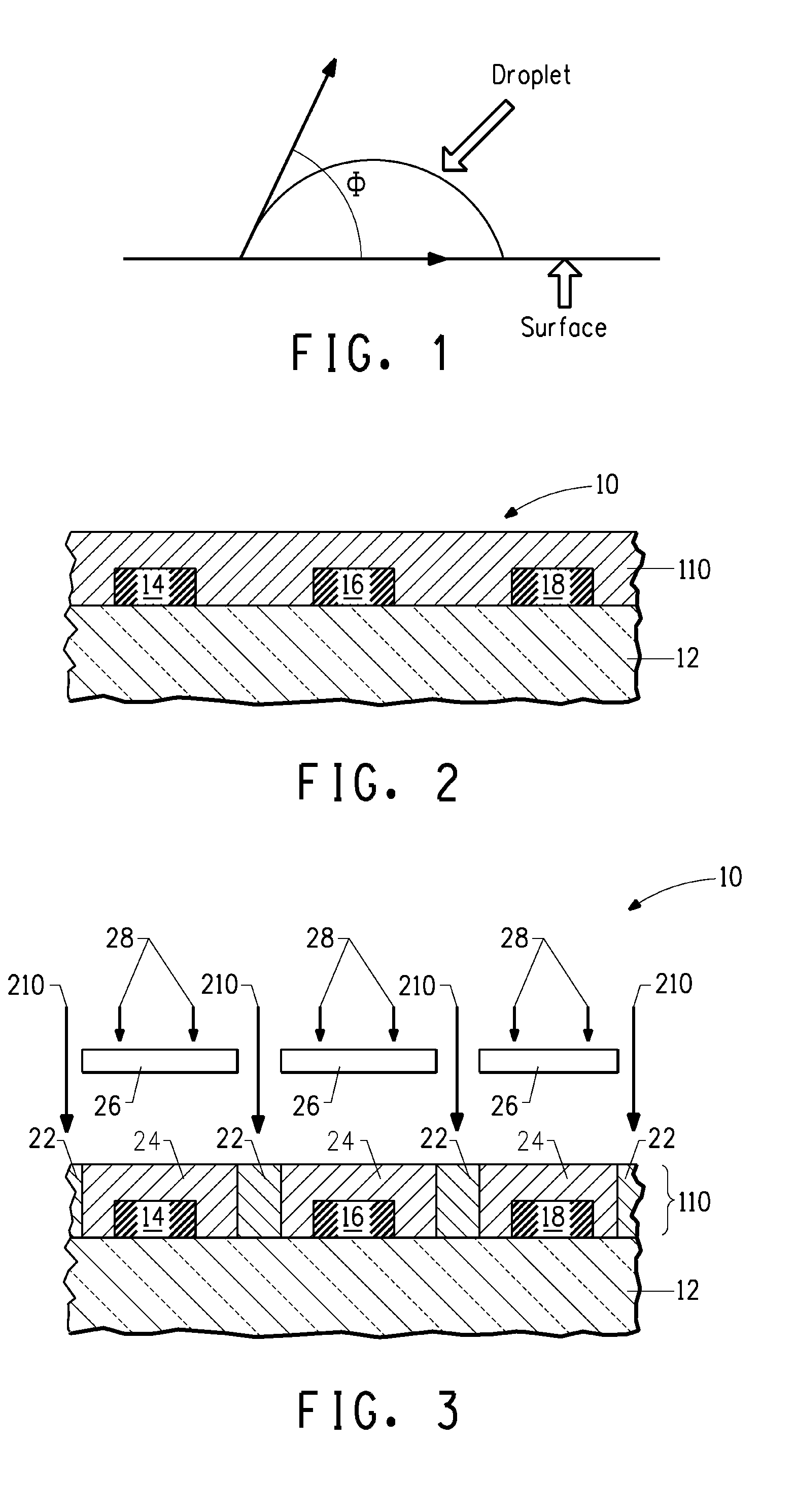
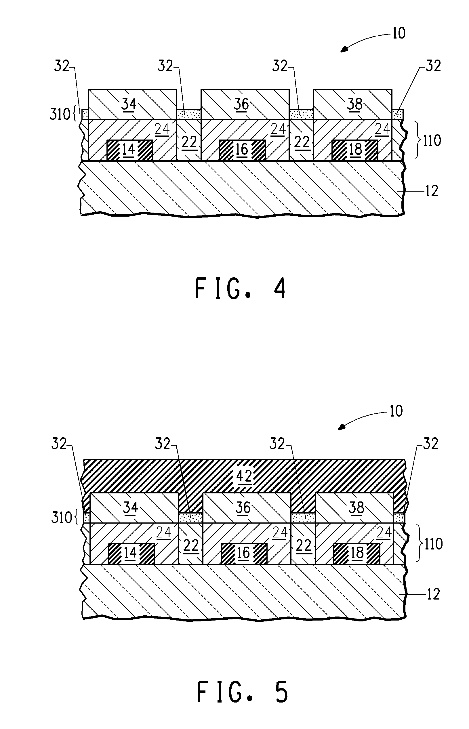
[0140]This example illustrates the process described herein where the resistivity of a hole-transport layer is increased, and the surface energy is decreased.

[0141]The hole-transport material is a crosslinkable copolymer of triphenylamine, dioctyl fluorene, and distyryl fluorene (“HT-1)”.

[0142]The radiation sensitizer is Darocur 1173 (Ciba Specialty Chemicals, Basel, Switzerland), which is an acetophenone derivative.

[0143]Backlight test displays will be made by coating sample solutions on to indium tin oxide coated glass substrates. Some of the displays will be exposed to UV light. The backlights will be baked at 275 C for 30 minutes to crosslink the HT-1, and simultaneously remove the Darocur 1173, if present. The backlights will be covered with appropriate cathode layers of ZrQ then LiF then Al by vapor deposition, and then encapsulated to exclude air and water vapor. The resulting diodes represent the structure of the leakage paths in an actual display. A voltage will be applied,...


PUM

PropertyMeasurementUnit
temperatureaaaaaaaaaa
wavelengthaaaaaaaaaa
wavelength of radiationaaaaaaaaaa

Abstract

A process of forming an electronic device is disclosed. An organic device layer is formed. The organic device layer includes a charge-selective material and a radiation sensitizer and has a first electrical conductivity and a first surface energy. First portions of the organic device layer are selectively exposed to radiation. The electrical conductivity and surface energy of the first portions of the organic device layer are modified.

Description

RELATED APPLICATION DATA[0001]This application claims priority under 35 U.S.C. § 119(e) from U.S. Provisional Application No. 61 / 013,197 filed on Dec. 12, 2007, which is incorporated by reference herein in its entirety.BACKGROUND INFORMATION[0002]1. Field of the Disclosure[0003]This disclosure relates in general to processes for forming organic electronic devices.[0004]2. Description of the Related Art[0005]Electronic devices, including organic electronic devices, continue to be more extensively used in everyday life. Forming circuits in such electronic devices includes forming conductive pathways in organic layers such as those that lie between electrodes of the electronic device. One method to define the conductive pathway is to form a conductive structure by removing portions of a previously formed conductive layer. Another method is to print the conductive structure using a selective deposition technique. Insulating material can be deposited between such conductive structures to...

Claims


Application Information

Patent Timeline
Patent Type & Authority Applications(United States)
IPC IPC(8): G03F7/20
CPCG03F7/0007G03F7/0046G03F7/0388H01L51/56H01L51/5048H01L51/5281H01L51/0018H10K71/233H10K50/14H10K50/86H10K71/00
Inventor LANG, CHARLES D.KOLOSOV, DMITRYTRUJILLO, JOHANN THOMAS
Owner LG CHEM LTD
Why Eureka
Try Eureka