Process for Making a Multilayer Circuit Device Having Electrically Isolated Tightly Spaced Electrical Current Carrying Traces

a technology of tightly spaced electrical current and multi-layer circuit boards, which is applied in the direction of ceramic shaping apparatus, electric devices, special surfaces, etc., can solve the problems of increasing the danger of accidental bridging adjacent pins with solder, affecting the signal quality of high-speed electronic circuits, and affecting the quality of electrical circuits

Inactive Publication Date: 2009-06-25
VERTICALTEST
View PDF9 Cites 56 Cited by
  • Summary
  • Abstract
  • Description
  • Claims
  • Application Information

AI Technical Summary

Problems solved by technology

As pin grid arrays and dual-in-line surface mount (SOIC) packages are produced with more and more pins, and with decreasing spacing between the pins, interfacing difficulties arise in connecting the integrated circuits to systems using the circuit device.
For example, as even modern package pins get closer together, the danger of accidentally bridging adjacent pins with solder increases.
Moreover, the shorter an electrical conductor between IC device and the system to which it is connected, the lower its inductance, a property which causes unwanted distortion of signals in high-speed electronic circuits.
However, as IC devices continue to include more and more I / Os it is not always convenient to use the standard I / O locations of even BGA packages for connecting an electronic device to a system using the device.
However, state of the art laser technology can not be utilized to produce trace spacings of less than about 25 microns; and3) PCB milling, which uses a two or three-axis mechanical milling system to mill away the copper foil from the substrate.
However, a problem with use of this method for small trace geometries is that the etching step undercuts the edges of the traces yielding undesirable results.
Moreover, since production efficiencies require that all die now be tested at the wafer level, it is no longer feasible to test each die individually, and accordingly, it is important that many die be simultaneously tested.
Disadvantages of stripline are two: first, it is much harder (and more expensive) to fabricate than microstrip.
Lumped-element and active components either have to be buried between the groundplanes (generally a tricky proposition), or transitions to microstrip must be employed as needed to make connections on the top of the board.
A second disadvantage of stripline is that because of the second groundplane, the strip widths are much narrower for a given impedance (such as 50 ohms) and board thickness than for microstrip.

Method used


Image

  • Process for Making a Multilayer Circuit Device Having Electrically Isolated Tightly Spaced Electrical Current Carrying Traces
  • Process for Making a Multilayer Circuit Device Having Electrically Isolated Tightly Spaced Electrical Current Carrying Traces
  • Process for Making a Multilayer Circuit Device Having Electrically Isolated Tightly Spaced Electrical Current Carrying Traces

Examples


Embodiment Construction

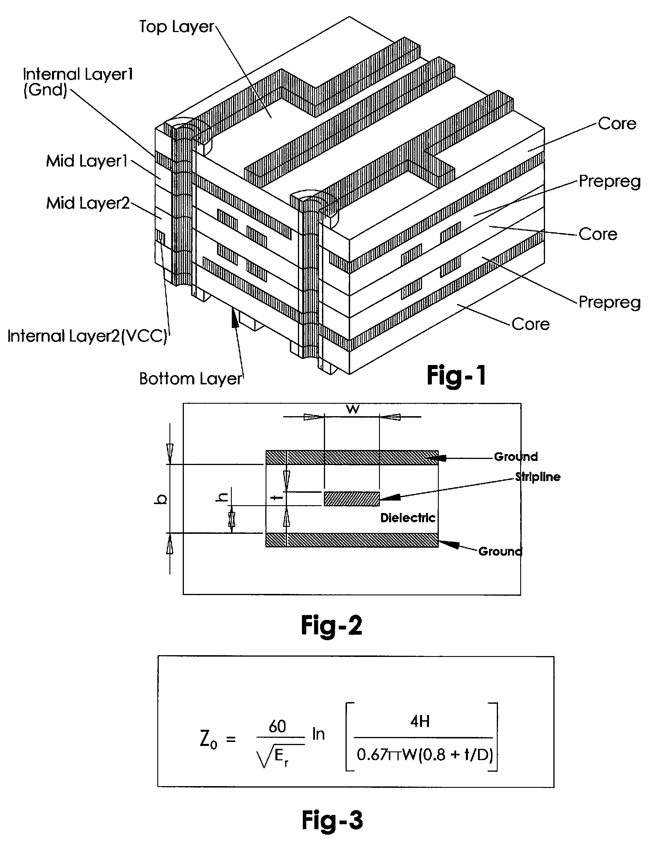
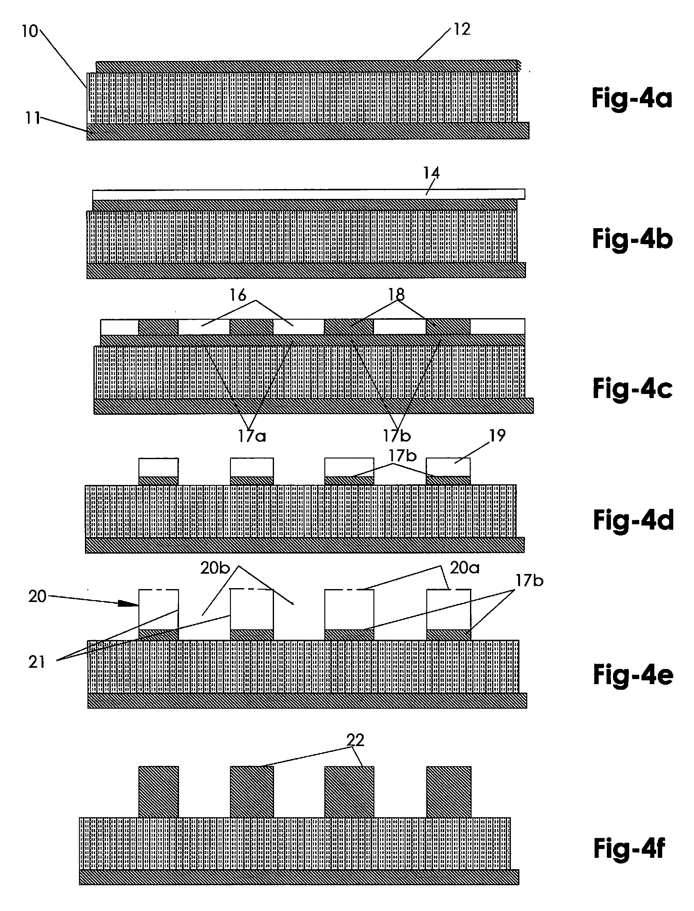
[0034]Referring now to FIG. 4a, a planar substrate is shown generally at 10 having a particular dielectric constant suitable for the application described. Board 10 may be of a ceramic material, a woven epoxy glass material known as FR4, or any other suitable substrate material. The substrate board may have a metal layer of a material such as copper plated on its bottom surface as indicated at 11

[0035]In accordance with a first embodiment of the present invention wherein circuit traces are to be provided by electroplating, a first step is to lay down a thin metallic seed layer 12 of a suitable material, such as copper or silver for example, on the upper surface of the substrate by printing, spraying, using an electroless process, etc. The seed layer 12 is a very thin plating of about 1 micron thickness with high conductive quality and good adherence to the substrate 10. This layer will serve as a foundation for the subsequent plating process.

[0036]The next step, as illustrated in FI...


PUM

PropertyMeasurementUnit
widthaaaaaaaaaa
dielectric constantaaaaaaaaaa
thicknessaaaaaaaaaa

Abstract

A process for making a multilayer circuit device having electrically isolated tightly spaced electrical current carrying traces, comprising of providing an insulative substrate having a first side coated with a layer of conductive metal intended to form a ground plane; providing a plurality of seed layer traces of a predetermined width of approximately 25 microns or less separated from each other by a predetermined distance of approximately 25 microns or less on a second side of the insulative substrate, the narrowness of such separation being essentially limited only by characteristics of the photoresist material to be deposited and developed therebetween and to withstand subsequent processing; developing ribs or barriers of photoresist forming vertical walls rising above the spaces separating the seed layer traces and defining valleys or channels thereover; depositing a desired thickness of conductive material over the seed layer traces and in the valleys or channels between the vertical walls; stripping away the resist ribs or barriers to leave conductive traces to be variously used as ground lines, signal lines and power lines; repeating the previous steps to develop a plurality of circuit boards; stacking the several circuit boards and joining them together with layers of insulative material; identifying particular ones of the traces as signal lines and other traces as power lines and/or ground lines; interconnecting at least some of the ground lines on one board to ground lines and/or ground planes on other boards by conductors extending through vias; interconnecting signal lines to signal input and output terminals; and perhaps to signal lines on other boards through vias; and interconnecting power lines to power input and output terminals, and perhaps to power lines on other boards through vias.

Description

[0001]This application is related to and incorporates by reference in its entirety the invention disclosures of U.S. patent application Ser. No. 11 / 890,222, and U.S. Provisional Applications Ser. No. 61 / 001,156 filed on Oct. 31, 2007, and Ser. No. 60 / 989,361 filed Nov. 20, 2007. Applicants claim priority to U.S. Provisional Applications Ser. No. 61 / 001,156 filed on Oct. 31, 2007FIELD OF THE INVENTION[0002]The present invention relates generally multilayer circuit apparatus and more particularly to a process for making a multi-layered circuit board having closely spaced circuit traces and particularly suited for use as a multi-circuit interface / connector device or a probe card transformer used to link an IC test system to probe pins or contactors used to engage the die pads or solder bumps or the like of IC devices before they are separated from the wafer upon which they are formed.BACKGROUND OF THE INVENTION[0003]A probe card assembly typically includes a contactor substrate carryin...

Claims


Application Information

Patent Timeline
Patent Type & Authority Applications(United States)
IPC IPC(8): H05K3/10H01S4/00
CPCH05K3/108Y10T29/49144H05K3/1258H05K3/243H05K3/4611H05K3/4623H05K2201/09318H05K2201/09536H05K2201/098H05K2203/013H05K2203/0568H05K2201/09327Y10T29/49165Y10T29/49124Y10T29/49002Y10T29/49155Y10T29/49126H05K3/125
Inventor NGUYEN, VINH T.HAMRICK, CLAUDE A.S.
Owner VERTICALTEST
Why Eureka
Try Eureka