

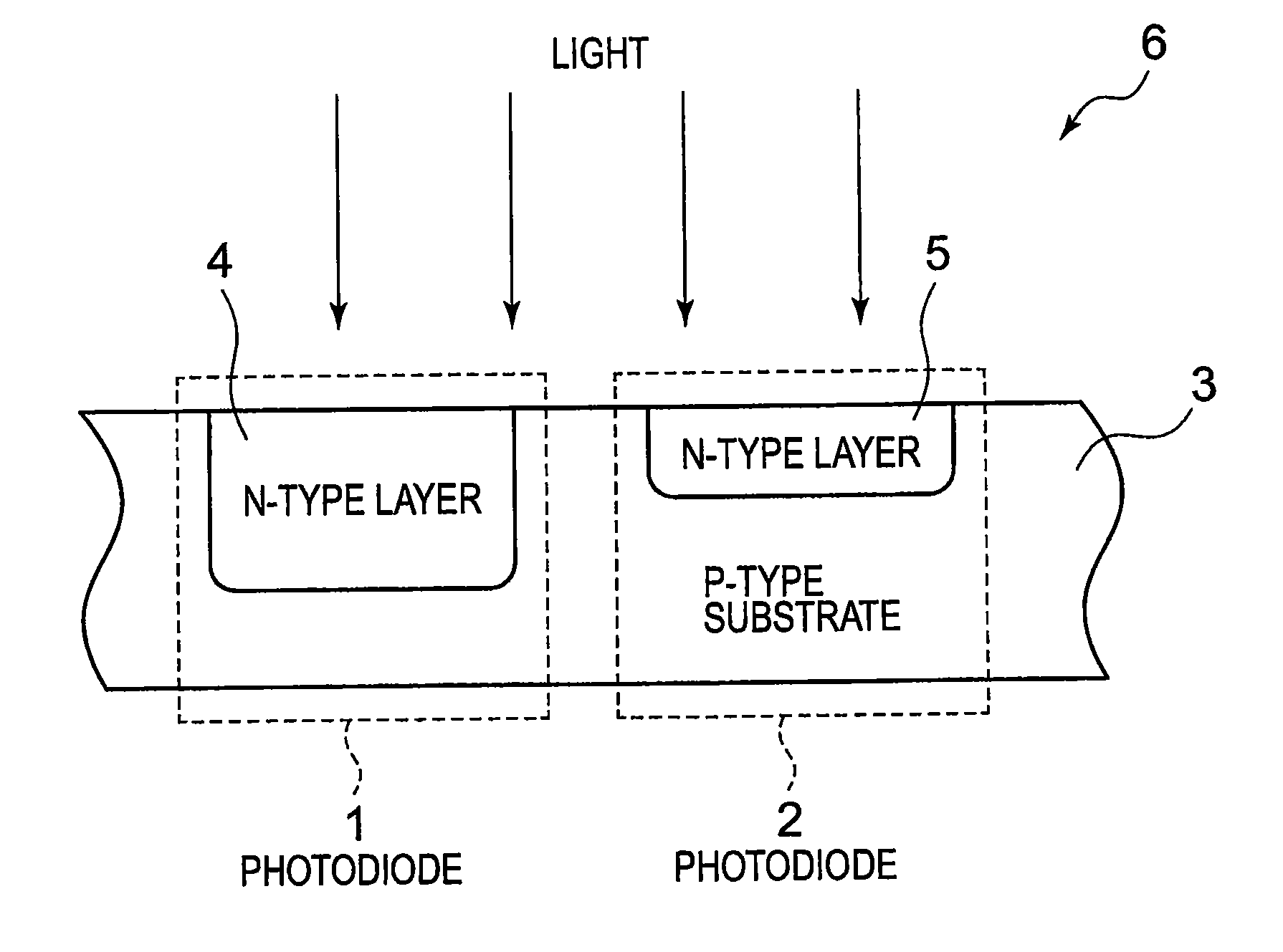
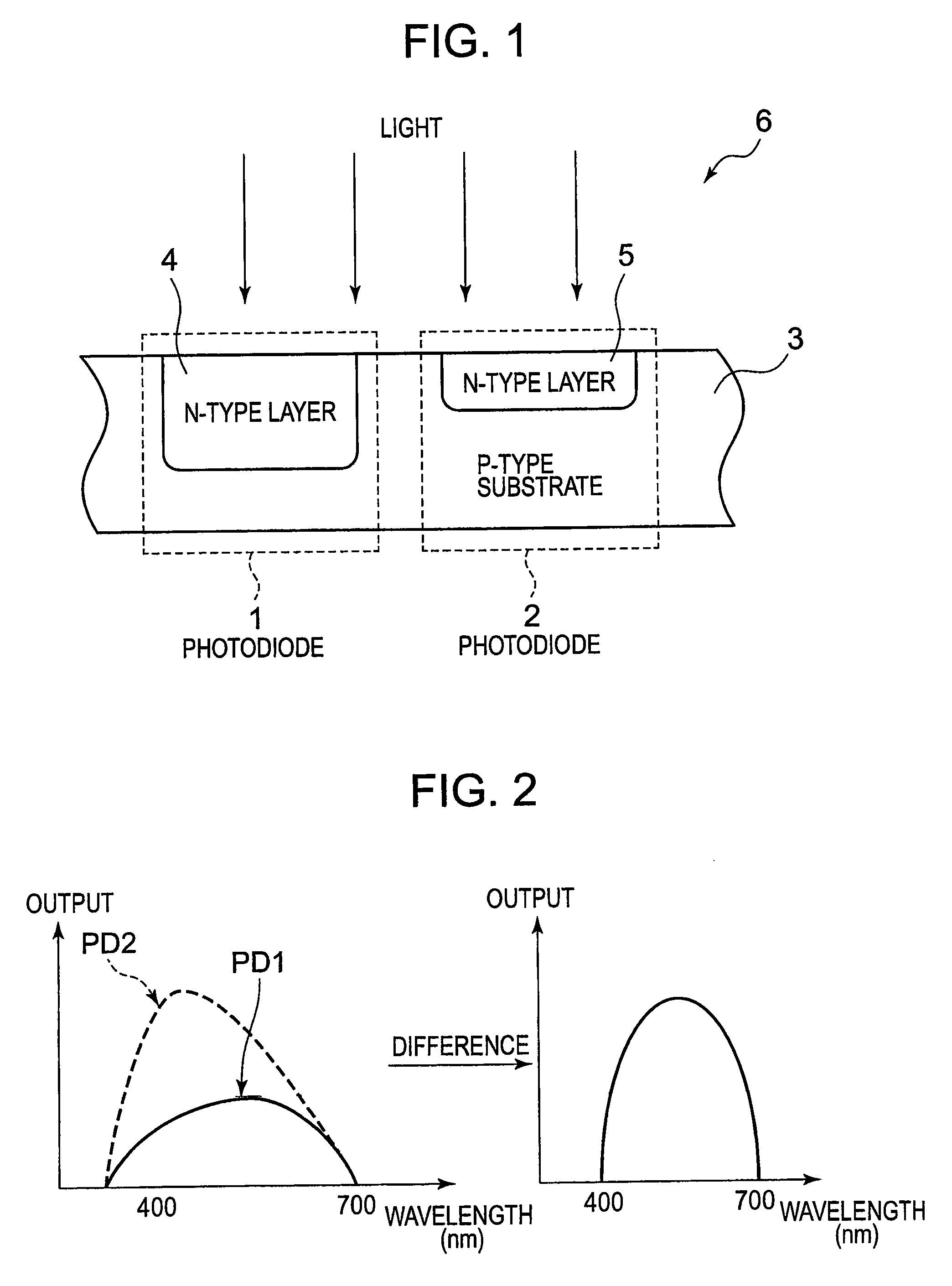
Photodetection semiconductor device, photodetector, and image display device
a semiconductor and photodetector technology, applied in the direction of radiation controlled devices, optical radiation measurement, instruments, etc., can solve the problem of affecting the detection value, and achieve the effect of reducing the influence of electromagnetic waves
- Summary
- Abstract
- Description
- Claims
- Application Information
AI Technical Summary
Benefits of technology
Problems solved by technology
Method used
Image

Examples
first modification
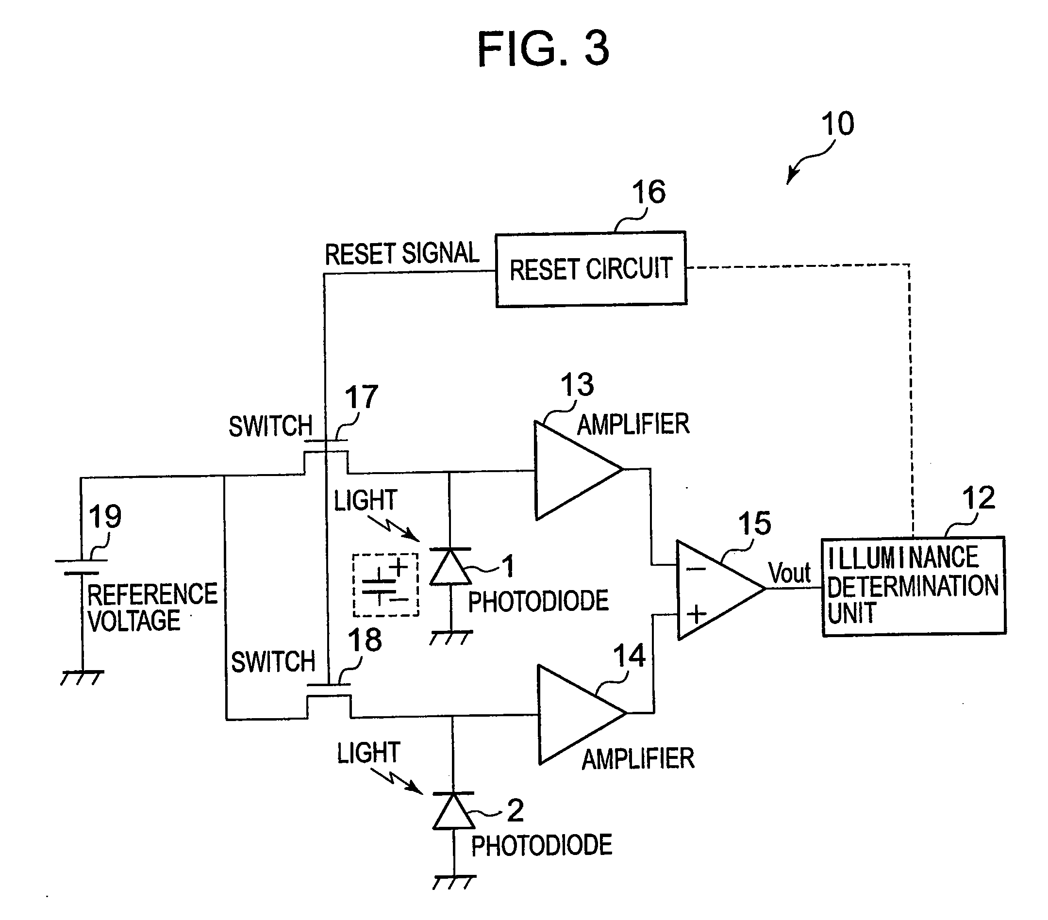
[0102]Receiving intense light causes rapid accumulation of the electric charges in the photodiodes 1 and 2, and hence large illuminance saturates the outputs of the photodiodes 1 and 2 before the detection of the output from the difference circuit 15 by the illuminance determination unit 12, thereby making incorrect measurement of a precise value.
[0103]In this modification, then, the reset interval is shortened against intense receiving light to shorten the accumulation period for the electric charge to prevent the saturation of the photodiodes 1 and 2, thereby permitting widening of the dynamic range.
[0104]FIG. 4A is a schematic graph for describing a case in which the output of the photodiode 2 is saturated at the time of reset.
[0105]First, when the switches 17 and 18 are turned off after connecting the photodiodes 1 and 2 to the DC power supply 19 to set the voltage at the cathode terminals to the reference voltage, the voltage at the cathode terminals begin to decrease as illust...
second modification
[0117]The amplifiers 13 and 14 and the difference circuit 15 of the photodetector 10 (FIG. 3) receive the power supply from a power supply (not shown) to conduct an amplification process and a difference process.
[0118]In this modification, the amplifiers 13 and 14 and the difference circuit 15 are not always driven, but are intermittently driven only when the illuminance determination unit 12 detects the difference between the photodiodes 1 and 2 for determination (that is, when needed) to save the power consumption.
[0119]FIG. 6 is a diagram illustrating the configuration of a photodetector 10b according to this modification. It should be noted that the same configurations as those of FIG. 3 are denoted by identical reference numerals, and their description is simplified or omitted. Further, for simplification of the drawing, the photodiode 2, the amplifier 14, and the switch 18 are omitted.
[0120]A photodetector 10b further includes a timer 31 and switches 32 and 33 in addition to t...
third modification
[0128]This modification is made to reduce an influence of flicker in a light source.
[0129]A light source such as a fluorescent lamp may repeat tuning on and off or flicker in a cycle of 50 [Hz] or 60 [Hz].
[0130]In the photodetector 10 (FIG. 3), when the light intensity of the light source in which flicker occurs is measured, the measured value of the illuminance differs depending on a position of an instant in a flicker at which the illuminance determination unit 12 detects the difference.
[0131]For example, a cellular phone is frequently used in a room, which is illuminated with a fluorescent lamp, and thus it is necessary to measure the light intensity appropriately under the presence of flicker.
[0132]In this modification, the difference between the photodiodes 1 and 2 is thus time-averaged to reduce the influence of flicker.
[0133]FIG. 7 is a diagram illustrating a configuration of a photodetector 10c that is designed with a countermeasure against flicker. The same configurations a...
PUM
 Abstract
Description
Claims
Application Information