
Fused thiophene acenes and organic semiconductors made therefrom

a technology of organic semiconductors and acenes, which is applied in the direction of non-metal conductors, instruments, conductors, etc., can solve the problems of poor device stability, high on/off ratios cannot be obtained in an inert atmosphere, and suffer from the performance of most of the above organic semiconductor compounds

Inactive Publication Date: 2009-07-02
EI DU PONT DE NEMOURS & CO
View PDF0 Cites 2 Cited by
  • Summary
  • Abstract
  • Description
  • Claims
  • Application Information

AI Technical Summary

Benefits of technology

[0014]Yet another embodiment provides light-emitting diodes, photo conductors, memory cells, current limiters, field-effect diodes, Schottky diodes, photovoltaic

Problems solved by technology

The performance of most of the above organic semiconductors compounds suffers from either low charge mobility (ca.
Pentacene compounds often show high oxygen and humidity sensitivity, and therefore high on / off ratios can only be obtained in an inert atmosphere.
These characteristics result in poor device stability and make pentacene compounds unsuitable for practical electronic circuit applications.
On the other hand, compounds such as oligofluorenes, oligofluorene-thiophenes, phenylene-thiophene, and conjugated polyfluorene-thiophene polymers show improved stability, but their low charge mobility limits their applications in high efficiency electronic devices.

Method used


Image

  • Fused thiophene acenes and organic semiconductors made therefrom
  • Fused thiophene acenes and organic semiconductors made therefrom
  • Fused thiophene acenes and organic semiconductors made therefrom

Examples


example 1

[0066]

[0067]Into a 500 mL round bottom flask, bromine (128 g, 0.8 mole) in acetic acid (200 mL) was added slowly over 0.5 h at room temperature to a solution of 2,7-dihydronaphthalene (32.0 g, 0.2 mole) dissolved in acetic acid (300 mL). An orange yellow precipitate was formed. This was stirred at 80° C. for 1 h. Then water (100 mL) was added, and the light yellow mixture was heated at 80° C. for an additional hour. Tin powder (48 g, 0.4 mol) was added in three portions (over about 10 min) and the mixture heated to reflux at 80° C. An off-white precipitate was formed. After 1 h, a light yellow clear solution was obtained. TLC (hexane:ethyl acetate=1:1) showed several products (Rf: 0.7, 0.65, 0.6 and 0.5 and 0.4). Rf=0.5 is the main product. Reflux was continued overnight until all the tin disappeared. Most of the solvent was evaporated and the residue was poured into water. The precipitate was collected by filtration. The solid was dissolved in ethyl acetate and the solvent was part...

example 2

Characterization of FET Devices

[0069]This Example summarizes results obtained for the characterization of FET devices that had a W / L ratio of 10, where W is the channel width and L is the channel length.

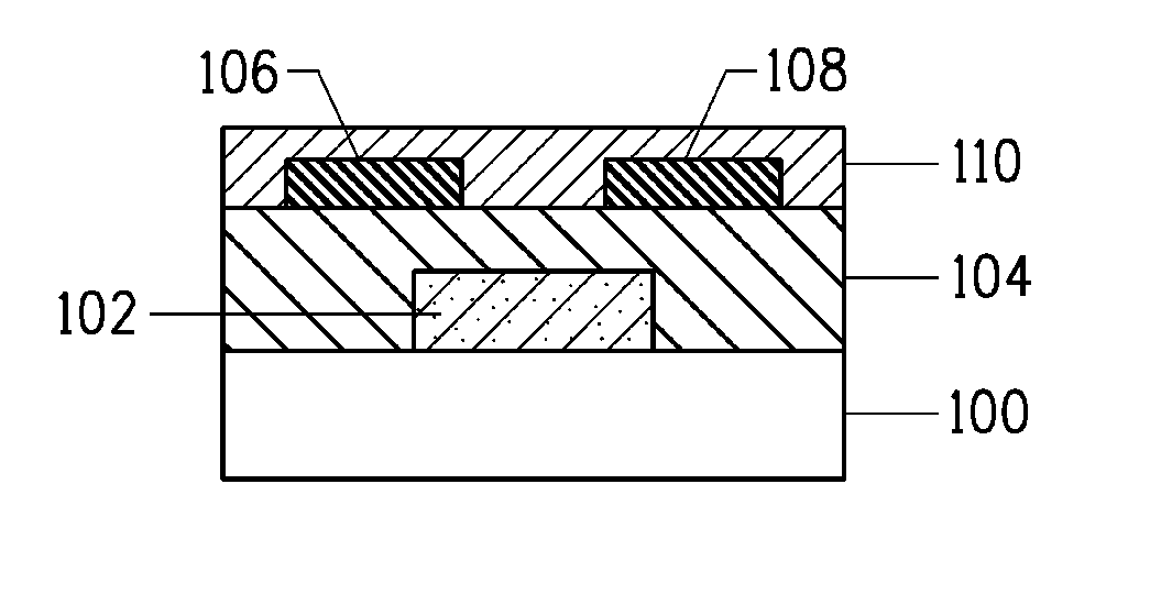
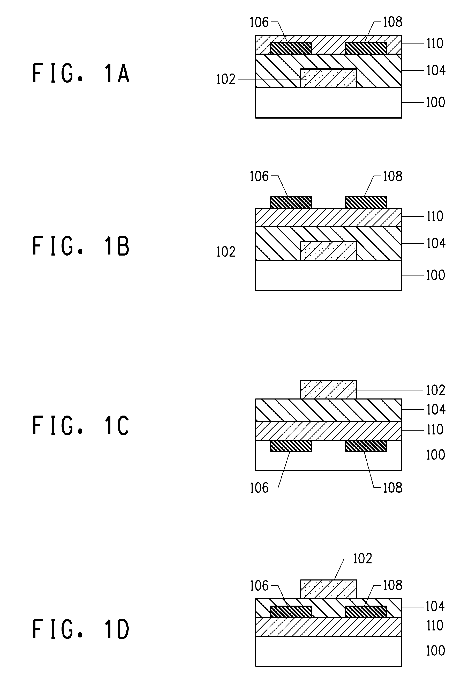
[0070]The FET devices were fabricated in a similar manner as described in conjunction with FIG. 1B. Thereafter, the performance of each FET device was characterized using an Agilent 4155C™ Semiconductor Parameter Analyzer interfaced with a probe station.

[0071]Measurements were made under ambient conditions, with no special precautions taken to control temperature, or to exclude light or air.

[0072]The results were obtained from the characterization of the OFET devices using compound 10 are summarized in the Table. These results show that solution processible OFET devices comprising compounds of Formula 1 have high mobilities and high on / off ratios.

TABLEOFET Device Characteristics of Compound 10 using solutionprocessDevice CharacteristicsSubstrateμsatVtsatSubThrSWsatSCTemperatureμlinOn...


PUM


Abstract

This invention relates to fused thiophene acene compounds and their use in organic semiconductors. The compounds exhibit useful electronic properties such as high mobility and high on / off ratio. The compounds can be used in electronic devices such as field effect transistors (FETs), display devices, light-emitting diodes, photovoltaic cells, photo-detectors, and memory cells. Also provided are methods for making the fused thiophene acenes.

Description

FIELD OF THE INVENTION[0001]The present invention relates to a new class of fused thiophene acene compounds. The invention also relates to electronic devices and methods of manufacturing the electronic devices using the thiophene acenes.BACKGROUND[0002]Organic materials have been widely used in electronic devices such as organic field-effect transistors (OFETs), light emitting diodes (OLEDs), photovoltaic diodes, and liquid crystal displays. OFETs are of special interest for use in low-cost integrated circuit (IC) technology suitable for applications such as smart cards, electronic tags, displays, and memory devices. In OFETs, the semiconductor layer consists of organic semiconductor materials including conjugated polymers and oligomers. Many organic materials possessing the required electronic properties for the electronic device applications have been synthesized.[0003]Organic compounds that have been investigated for use as semiconductors include conjugated polymers such as regio...

Claims


Application Information

Patent Timeline
IPC IPC(8): H01B1/12C07D495/22
CPCB82Y10/00Y02E10/549C09K11/06C09K2211/1007C09K2211/1011C09K2211/1092G11C13/0014G11C13/0016G11C13/025H01L51/0074H01L51/0541H01L51/0545H01L51/5012H05B33/14C07D495/22H10K85/6576H10K10/464H10K10/466H10K50/11
Inventor MENG, HONGSUN, FANGPING
Owner EI DU PONT DE NEMOURS & CO
Learn More