Field Effect Transistor

a field effect transistor and transistor technology, applied in the direction of basic electric elements, electrical equipment, semiconductor devices, etc., can solve problems such as destabilization of operations, and achieve the effects of improving device characteristics, improving source resistivity, and improving the breakdown voltage of gates

Inactive Publication Date: 2009-07-09
NEC CORP
View PDF4 Cites 17 Cited by
  • Summary
  • Abstract
  • Description
  • Claims
  • Application Information

AI Technical Summary

Benefits of technology

[0039]In the field effect transistor of the present invention, in the sectional view taken along the direction of gate length, the side wall of the recess and the side wall of the gate electrode both on the source electrode side and on the drain electrode side thereof may be brought into direct contact with each other. This configuration may further improve the source resistivity, and may improve the device characteristics.
[0040]In the field effect transistor of the present invention, the gate electrode may completely fill up the recess.
[0041]In the field effect transistor of the present invention, the gate electrode may have a field plate portion formed on the insulating film as being swelled out thereon towards the drain electrode side like a penthouse. By virtue of this configuration, concentration of electric field at the drain-side end of the gate electrode may more effectively be moderated. Therefore, the breakdown voltage of gate may further be improved.
[0042]In the present invention, an insulating film having a low interfacial level density may be adoptable as the insulating film provided over the second undoped GaN layer in the region other than the vicinity of the gate electrode. By virtue of this configuration, the collapse possibly occurs between the gate electrode and the drain electrode may further effectively be suppressed. This sort of insulating film may specifically be exemplified by nitrogen-containing insulating film, and further specifically by SiN film, SiON film and SiCN film. In this way, the transistor reduced in the collapse and gate leakage current, and further suitable for higher output configuration, may be obtained.
[0043]In the present invention, the gate electrode may have a T-form, or Y-form. By virtue of this configuration, the gate resistivity may be reduced, the gain may be increased, and thereby the high-frequency characteristics may further be improved.
[0044]As is clear from the explanation in the above, the present invention may realize a transistor excellently balanced between the collapse and the breakdown voltage of gate.

Problems solved by technology

The collapse may occasionally produce hysteresis in the I-V characteristics, and may possibly destabilize the operations.

Method used


Image

  • Field Effect Transistor
  • Field Effect Transistor
  • Field Effect Transistor

Examples


Embodiment Construction

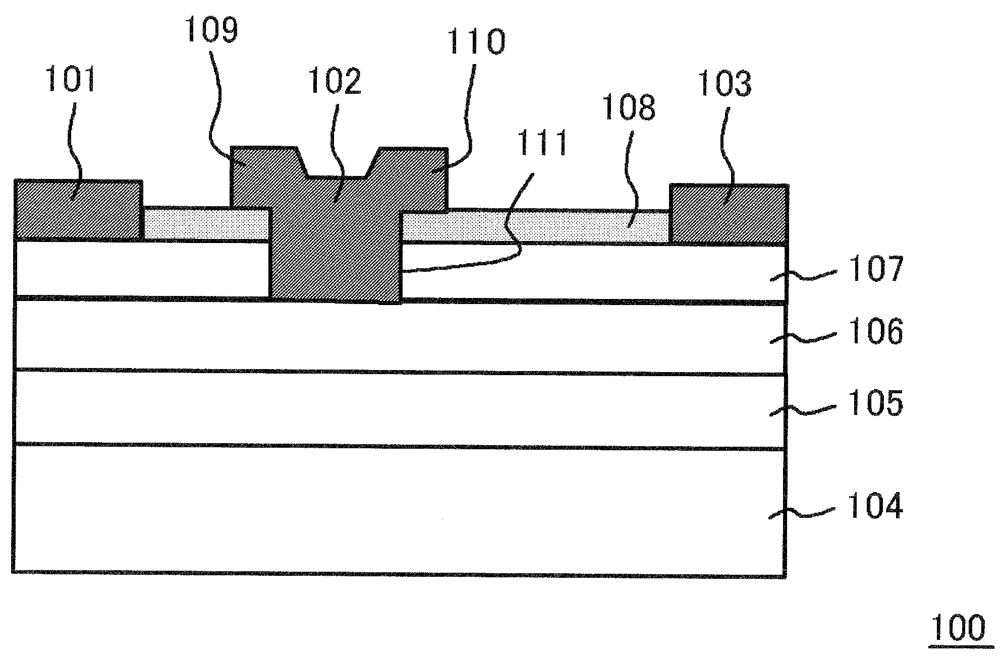
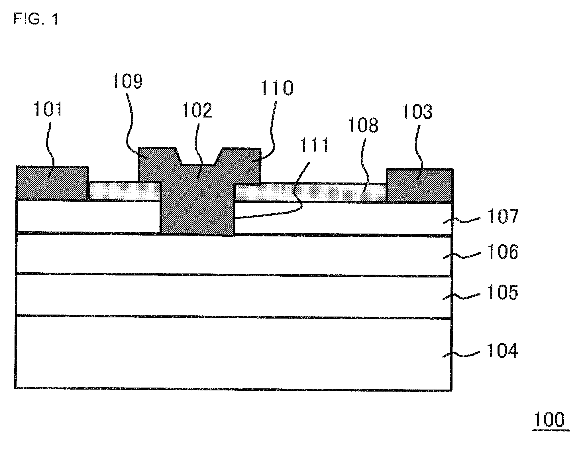
[0055]Embodiments of the present invention will be explained below, referring to the attached drawings. It is to be noted that any common constituents will be given with same reference numerals in all drawings, so that the explanations therefor will not be repeated for the convenience' sake. In this specification, all stacked structures will be expressed as “upper layer / lower layer (substrate side)”.

[0056]FIG. 1 is a sectional view showing a configuration of a compound semiconductor device. A semiconductor device 100 is a hetero-junction field effect transistor using a nitride-base Group III-V compound semiconductor for the channel layer.

[0057]The semiconductor device 100 has a Group III nitride semiconductor structure composed of an undoped GaN (i-GaN) channel layer 105, an AlGaN electron donor layer 106 provided over the undoped GaN channel layer 105 as being brought into contact therewith, and an undoped GaN (i-GaN) layer 107 provided over the AlGaN electron donor layer 106 as be...


PUM


Abstract

A semiconductor device 100 contains an undoped GaN channel layer 105, an AlGaN electron donor layer 106 provided on the undoped GaN channel layer 105 as being brought into contact therewith, an undoped GaN layer 107 provided on the AlGaN electron donor layer 106, a source electrode 101 and a drain electrode 103 provided on the undoped GaN layer 107 as being spaced from each other, a recess 111 provided in the region between the source electrode 101 and the drain electrode 103, as being extended through the undoped GaN layer 107, a gate electrode 102 buried in the recess 111 as being brought into contact with the AlGaN electron donor layer 106 on the bottom surface thereof, and an SiN film 108 provided on the undoped GaN layer 107, in the region between the gate electrode 102 and the drain electrode 103.

Description

TECHNICAL FIELD[0001]The present invention relates to a field effect transistor using Group III nitride semiconductors.BACKGROUND ART[0002]In recent years, electronic devices having an AlGaN (upper layer) / GaN (lower layer (substrate side) ) structure have more extensively been developed. The AlGaN / GaN structure has high voltage breakdown characteristics by virtue of its wide band gap characteristics, and are discussed to be applied in particular for high-frequency / high-output devices operated under higher voltages, and inverter power sources.[0003]There is known a conventional hetero-junction transistor having the AlGaN / GaN structure, described in Patent Document 1. FIG. 2 is a schematic sectional view showing a basic configuration of transistor described in the document.[0004]The transistor shown in FIG. 2 is manufactured by the procedures below.[0005]First, over a high-resistivity SiC substrate 24, an undoped GaN (i-GaN) channel layer 25 which serves as a channel layer and an AlGa...

Claims


Application Information

Patent Timeline
Patent Type & Authority Applications(United States)
IPC IPC(8): H01L29/205
CPCH01L29/2003H01L29/7787H01L29/66462
Inventor MATSUNAGA, KOUJIOTA, KAZUKIOKAMOTO, YASUHIRONAKAYAMA, TATSUOWAKEJIMA, AKIOANDO, YUJIMIYAMOTO, HIRONOBUINOUE, TAKASHIMURASE, YASUHIRO
Owner NEC CORP
Why Eureka
Try Eureka