

Monolithically-Integrated Graphene-Nano-Ribbon (GNR) Devices, Interconnects and Circuits
a graphene-nano-ribbon, monolithic integration technology, applied in the direction of logic circuits using specific components, nanoinformatics, pulse techniques, etc., can solve the problem of intrinsic ambipolarity of undoped graphene devices
- Summary
- Abstract
- Description
- Claims
- Application Information
AI Technical Summary
Problems solved by technology
Method used
Image

Examples
first embodiment
Application of Graphene Nanoribbons to Electronic Devices
Introduction
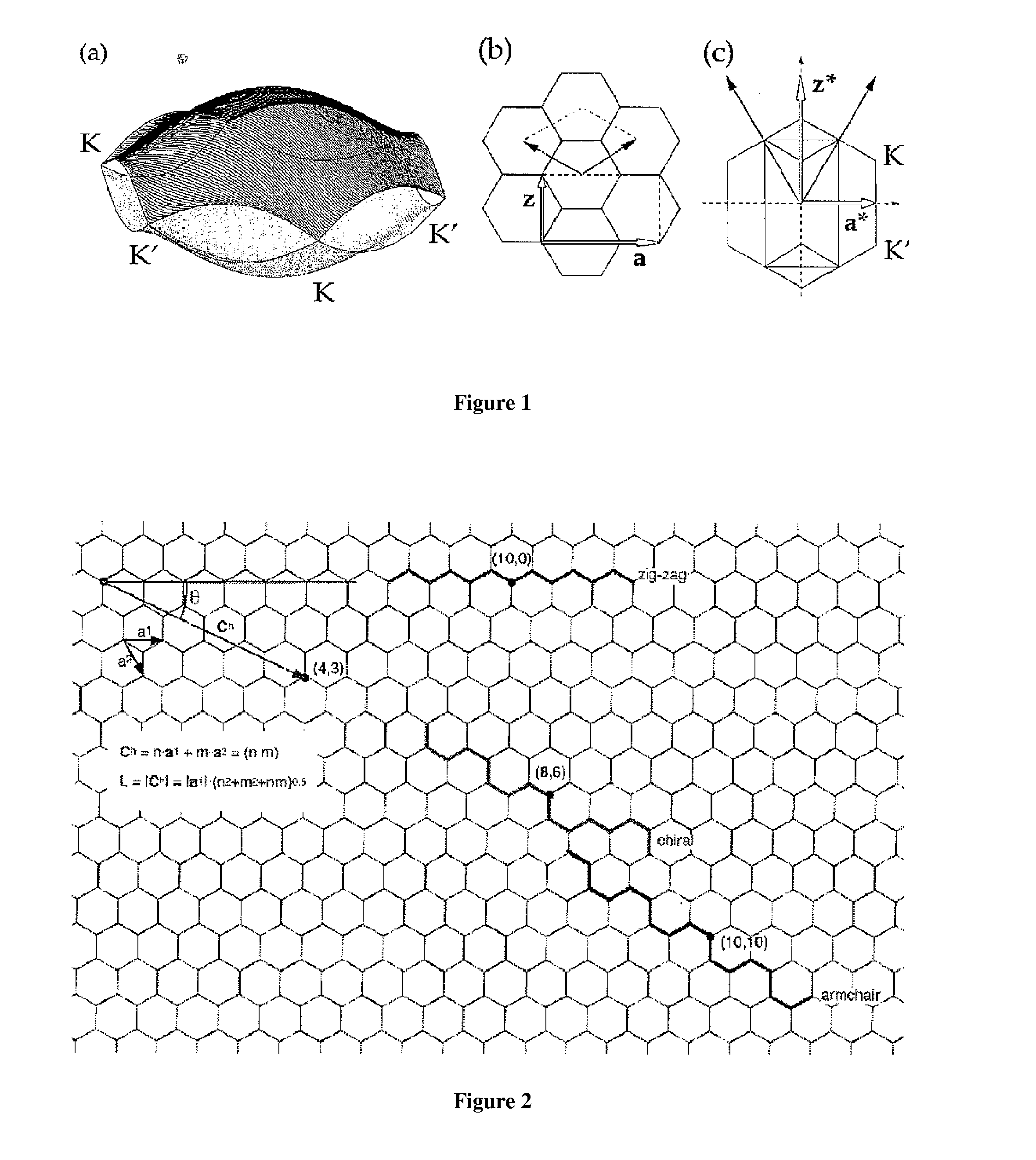
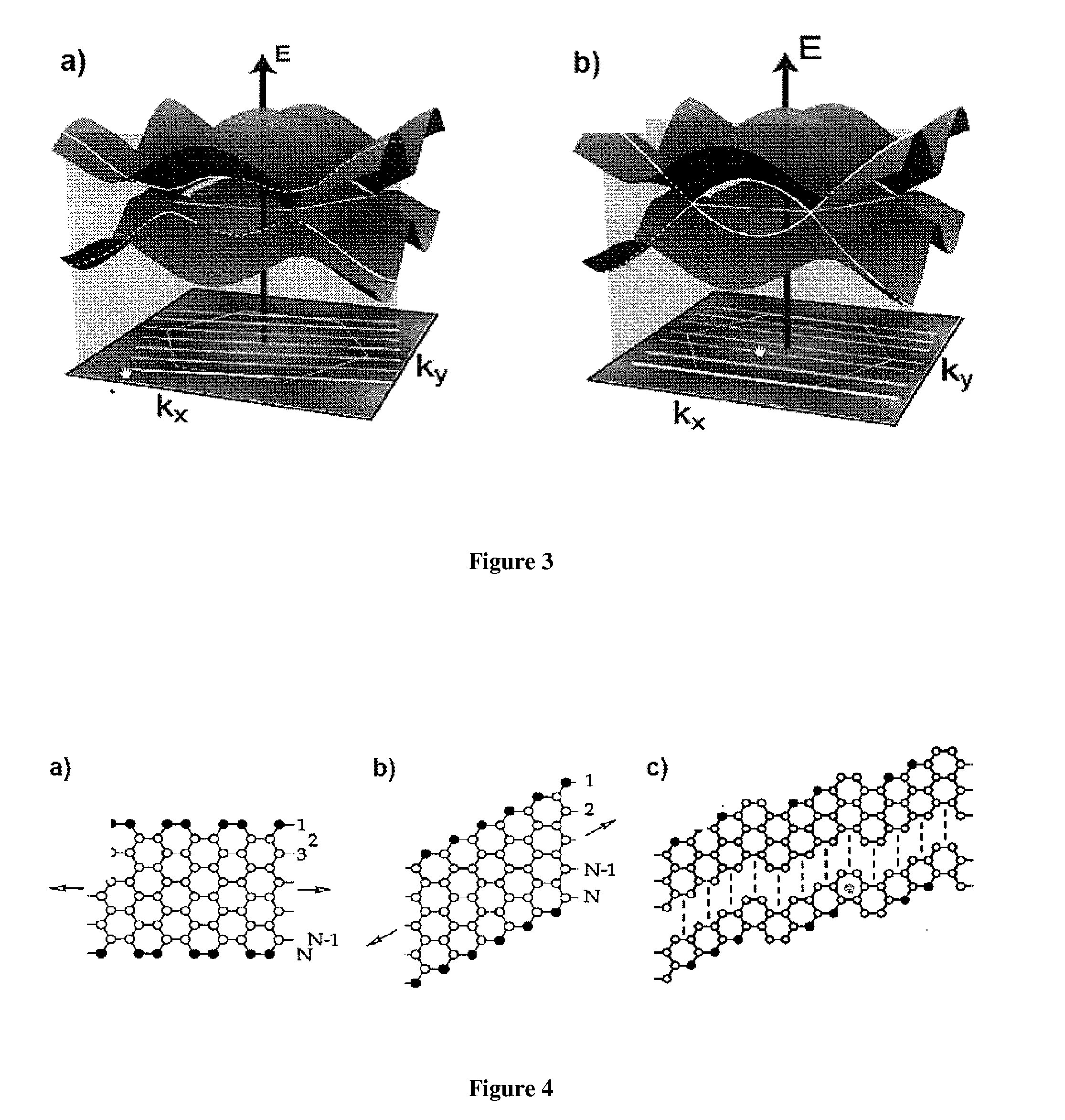
[0099]Graphene nanoribbons (GNRs), a term intended in this specification to encompass carbon nanoribbons (CNRs), are essentially a monolayer of graphite patterned into a narrow strip, and have recently been proposed as an attractive alternative to carbon nanotubes (CNTs) (see Background reference [63]). While CNTs have many highly desirable electronic properties (such as exceedingly high mobility and potentially excellent short channel effects in field-effect transistors (FETs) due to a small “depth” / length aspect ratio), no method of assembling large-scale circuits comprised of CNTs has yet been devised. The main difficulty is that CNTs are created prior to integration and need to be placed in correct positions in the circuit. This is contrary to the conventional planar process in silicon, in which devices are formed on the entire wafer at once by lithographic means. GNRs offer the promise of lithographic patterna...
second embodiment
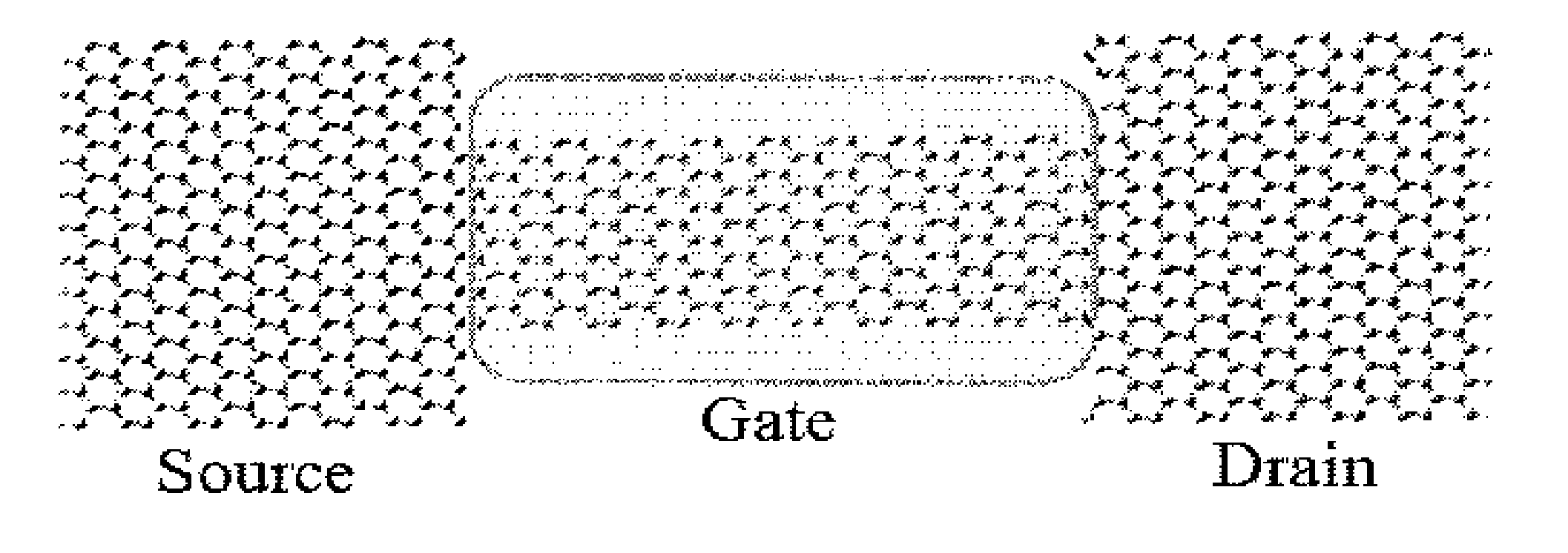
GNR-Based Transistor
[0144]This embodiment discloses a transistor based on graphene nanoribbons (GNRs), said switch having a substrate, said graphene originating from a continuous graphene sheet, said GNRs derived from said sheet using planar techniques, comprising: a conductive source GNR disposed on a substrate, wherein said source GNR is substantially metallic, and wherein said source GNR edges are zigzag-type, jagged-type, or armchair-type; a conductive drain GNR disposed on said substrate and spaced apart from the source, wherein said drain GNR is substantially metallic, and wherein said drain GNR edges are zigzag-type, jagged-type, or armchair-type; a semiconducting GNR disposed on said substrate having a variable resistance electrically connected between said source GNR and said drain GNR, wherein said semiconducting GNR is disposed between said source GNR and said drain GNR, and wherein said semiconducting GNR edges are armchair-type; and a conductive gate GNR disposed on sai...
third embodiment
GNR NOT Gate
[0149]This embodiment discloses a NOT gate based on graphene nanoribbons (GNRs), said gate having a substrate, said graphene originating from a continuous graphene sheet, said GNRs derived from said sheet using planar techniques, comprising: a conductive source GNR disposed on a substrate, wherein said source GNR is substantially metallic, and wherein said source GNR edges are zigzag-type, jagged-type, or armchair-type; a conductive drain GNR disposed on said substrate and spaced apart from the source, wherein said drain GNR is substantially metallic, and wherein said drain GNR edges are zigzag-type, jagged-type, or armchair-type; a semiconducting GNR disposed on said substrate electrically connected between said source GNR and said drain GNR, wherein said semiconducting GNR has two operational states, the first state being ON and the second state being OFF, wherein said semiconducting GNR has armchair edging, and wherein said semiconducting GNR is physically disposed in...
PUM
 Abstract
Description
Claims
Application Information