Method of Etching a High Aspect Ratio Contact

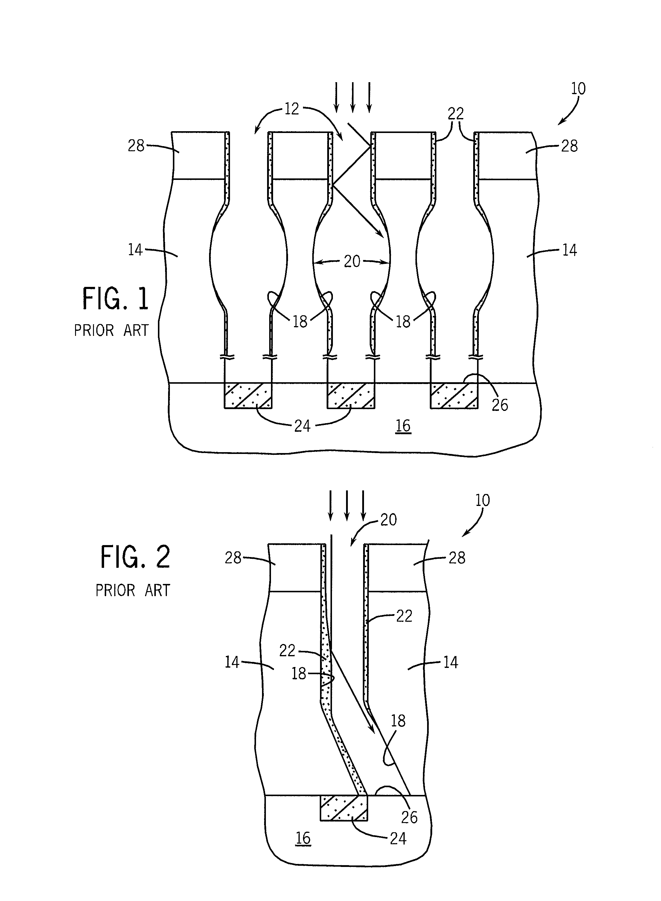
a high aspect ratio, contact technology, applied in the direction of surface treatment compositions, decorative arts, chemistry apparatus and processes, etc., can solve the problems of non-vertical contact holes, shortening the contact to an adjacent contact or other structure, and difficult control

Active Publication Date: 2009-07-09
MICRON TECH INC
View PDF36 Cites 120 Cited by
  • Summary
  • Abstract
  • Description
  • Claims
  • Application Information

AI Technical Summary

Problems solved by technology

However, such control is difficult when using conventional fluorocarbon chemistries.
Deviations such as bowing and twisting can also result in a non-vertical contact hole and shorting of the contact to an adjacent contact or other structure.

Method used


Image

  • Method of Etching a High Aspect Ratio Contact
  • Method of Etching a High Aspect Ratio Contact
  • Method of Etching a High Aspect Ratio Contact

Examples


Embodiment Construction

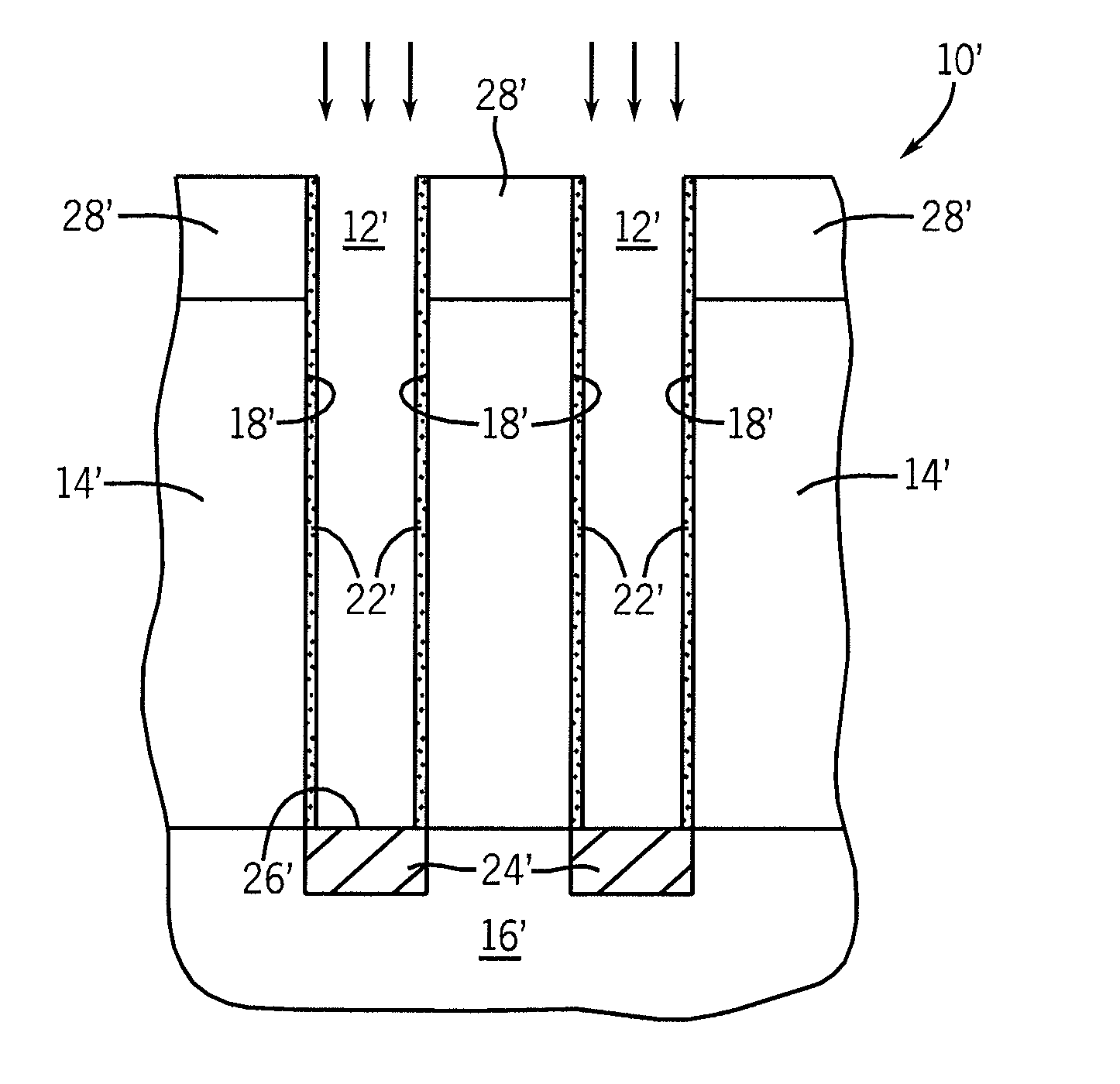
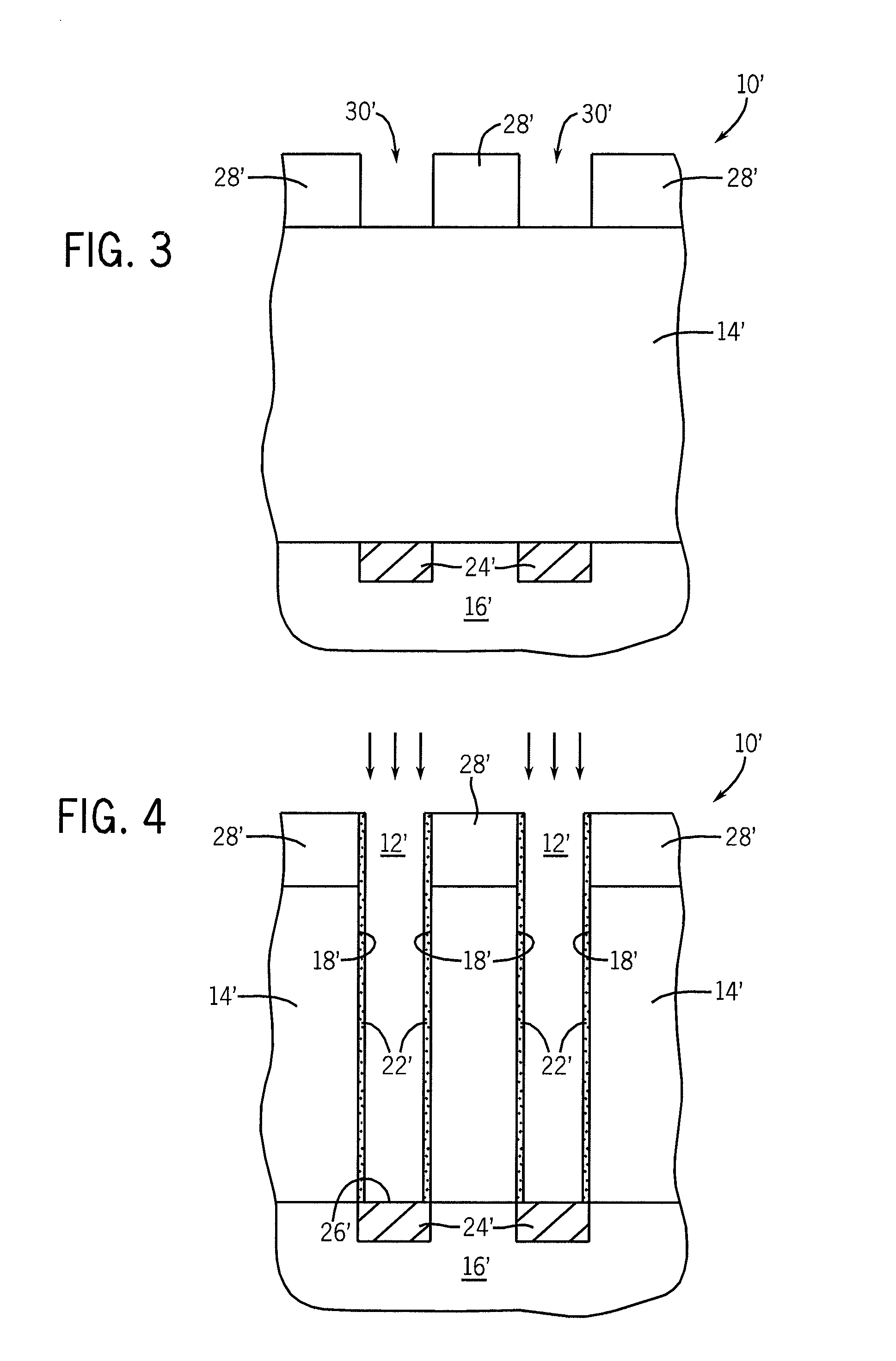
[0012]The following description with reference to the drawings provides illustrative examples of devices and methods according to embodiments of the invention. Such description is for illustrative purposes only and not for purposes of limiting the same.

[0013]In the context of the current application, the term “semiconductor substrate” or “semiconductive substrate” or “semiconductive wafer fragment” or “wafer fragment” or “wafer” will be understood to mean any construction comprising semiconductor material, including but not limited to bulk semiconductive materials such as a semiconductor wafer (either alone or in assemblies comprising other materials thereon), and semiconductive material layers (either alone or in assemblies comprising other materials). The term “substrate” refers to any supporting structure including, but not limited to, the semiconductive substrates, wafer fragments or wafers described above.

[0014]As used herein, the term “high-aspect ratio” refers to depth-to-wid...


PUM

PropertyMeasurementUnit
aspect ratioaaaaaaaaaa
depthaaaaaaaaaa
depthaaaaaaaaaa

Abstract

Methods and an etch gas composition for etching a contact opening in a dielectric layer are provided. Embodiments of the method use a plasma generated from an etch gas composed of C4F8 and / or C4F6, an oxygen source, and a carrier gas in combination with tetrafluoroethane (C2F4) or a halofluorocarbon analogue of C2F4.

Description

TECHNICAL FIELD[0001]Embodiments of the invention relate to gas chemistries and methods of plasma etching high aspect ratio contacts (HARCs) in oxide layers.BACKGROUND OF THE INVENTION[0002]In semiconductor devices, insulating layers such as silicon dioxide (SiO2), doped oxide such as BPSG, and silicon nitride, are used to electrically separate conductive layers, such as doped polysilicon, metals, refractory metal silicides, etc. High aspect ratio contact (HARC) etching is a key process for forming contact hole interconnections through insulating layers to an active device area or conductive layer in high density integrated devices. HARCs require etching processes that produce a vertical profile and a defined critical dimension (CD). Another application for HARC features in dielectrics is the formation of capacitor or container structures in stacked capacitor DRAM.[0003]In a typical plasma etching, a substrate is positioned on a chuck in a gas chamber, an etchant gas is introduced i...

Claims


Application Information

Patent Timeline
Patent Type & Authority Applications(United States)
IPC IPC(8): H01L21/3065C09K13/00
CPCC09K13/00H01L21/31116
Inventor BENSON, RUSSELL A.TAYLOR, TEDKIEHLBAUCH, MARK
Owner MICRON TECH INC
Why Eureka
Try Eureka