Process for producing air gaps in microstructures
a microstructure and air gap technology, applied in the field of microstructure air gap production process, can solve the problems of embrittlement of membranes, exposing them to serious degradation risks, and inability to integrate such membranes into microstructures, especially into air gap interconnect structures for integrated circuits
- Summary
- Abstract
- Description
- Claims
- Application Information
AI Technical Summary
Problems solved by technology
Method used
Image
Examples
example 1
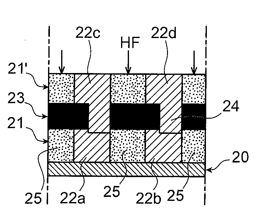
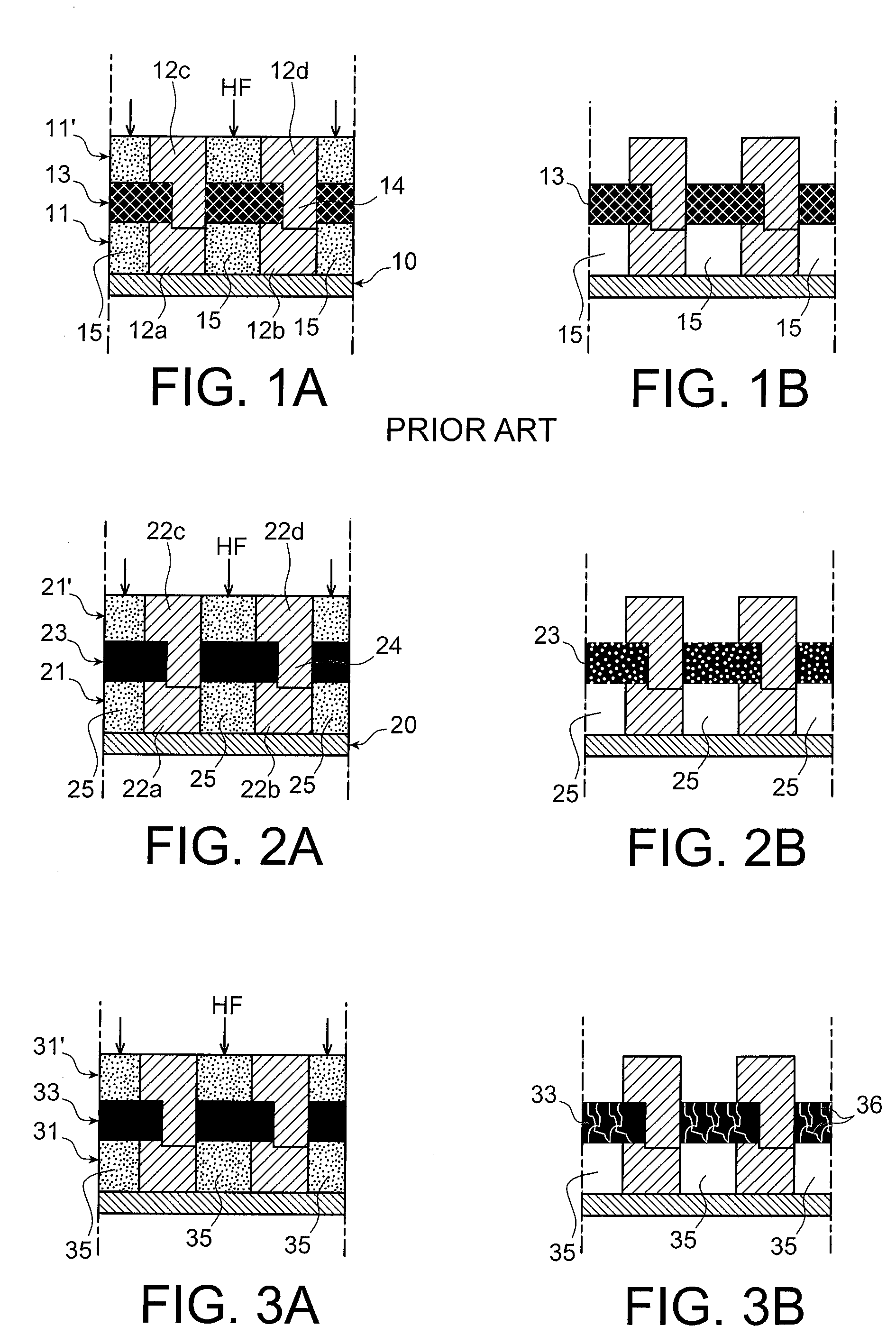
[0060]Reference is firstly made to FIGS. 2A and 2B which illustrate, in schematic form, a first example of how to implement the process of the invention in order to produce air gaps in an interconnect structure for integrated circuits.
[0061]In this example, the sacrificial material is silicon oxide while the impermeable membrane is an SivCwNxHyOz membrane (where v, w, x, y and z are all different from 0) which has an oxygen content of around 10 at % and a thickness of 200 nm.
[0062]Firstly, the structure shown in FIG. 2A comprising SiO2-filled cavities 25 is produced.
[0063]To do this, a first level of interconnects is produced on a suitable semiconductor substrate, typically made of silicon, said interconnects comprising metal lines 22a and 22b, typically made of copper, which are embedded in an SiO2 first layer 21. This first level of interconnects may be produced using a conventional route, i.e. for example by:
[0064]deposition of an SiO2 layer 21 on the substrate;
[0065]definition o...
example 2
[0083]Reference is now made to FIGS. 3A and 3B which illustrate schematically a second example of how to implement the process of the invention in order to produce air gaps in an interconnect structure for integrated circuits, which differs from that described in Example 1 only by the nature of the impermeable membrane integrated into the structure.
[0084]Specifically, in the present example, the impermeable membrane 33 consists of an amorphous hydrogenated silicon carbide (a-SiC:H) matrix, 200 nm in thickness, in which SiO2 through-nanowires are dispersed.
[0085]To obtain this membrane, the SiO2 nanowires are firstly formed on the first level of interconnects of the structure.
[0086]To do this, a first solution is prepared by gradually adding 52 ml of tetraethylorthosilicate (TEOS) to 115 mL of ethanol and a second solution is prepared by mixing 115 mL of ethanol with 18 mL of water and 0.27 mL of hydrochloric acid. The second solution is then added to the first. The resulting mixture...
PUM
| Property | Measurement | Unit |
|---|---|---|
| temperatures | aaaaa | aaaaa |
| dielectric constant | aaaaa | aaaaa |
| radio frequency | aaaaa | aaaaa |
Abstract
Description
Claims
Application Information

