Method To Control Semiconductor Device Overlay Using Post Etch Image Metrology

Inactive Publication Date: 2009-07-23
GLOBALFOUNDRIES INC
View PDF49 Cites 33 Cited by
  • Summary
  • Abstract
  • Description
  • Claims
  • Application Information

AI Technical Summary

Benefits of technology

[0013]It is another object of the present invention to provide a lithographic alignment method that reduces alignment error due to bias resulting from process-induced shifts in the post-develop overlay measurements relative to

Problems solved by technology

However, a drawback to using post lithography data is that the measurements can be readily biased by previous processing of the wafers.
It has been found that specific process layers are susceptible to process-induced shifts in the post-develop overlay measurements relative to the true overlay; e.g. chemical-mechanical polishing (CMP) smearing of overlay marks, asymmetric mark fill, asymmetric resist coating, and the like.
This bias, which frequently fits the modeled parameters, is then fed back to the lithography tool on subsequent lots resulting in an alignment error.
Thi

Method used


Image

  • Method To Control Semiconductor Device Overlay Using Post Etch Image Metrology
  • Method To Control Semiconductor Device Overlay Using Post Etch Image Metrology
  • Method To Control Semiconductor Device Overlay Using Post Etch Image Metrology

Examples


Embodiment Construction

)

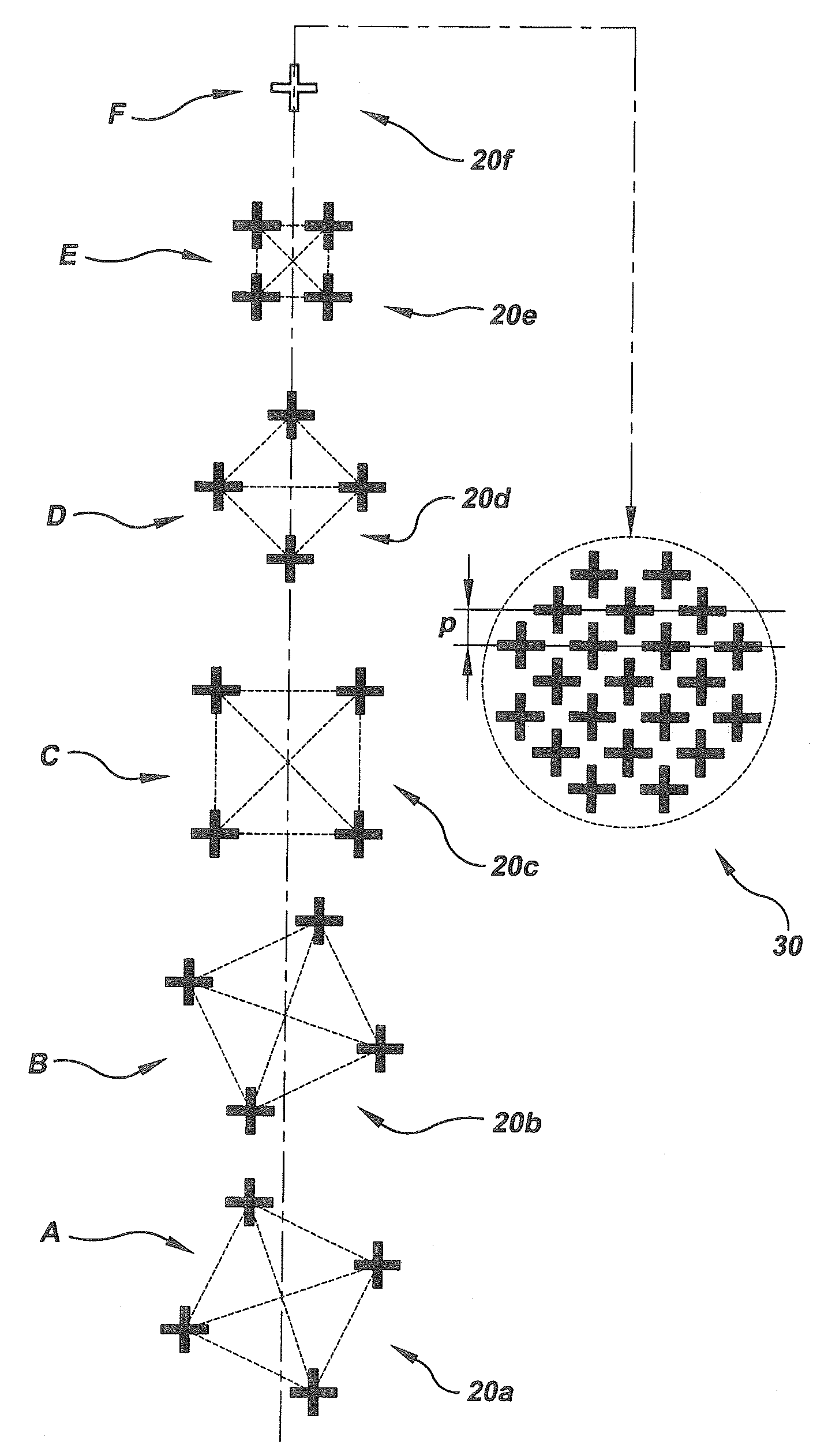
[0028]In describing the preferred embodiment of the present invention, reference will be made herein to FIGS. 1-5 of the drawings in which like numerals refer to like features of the invention.

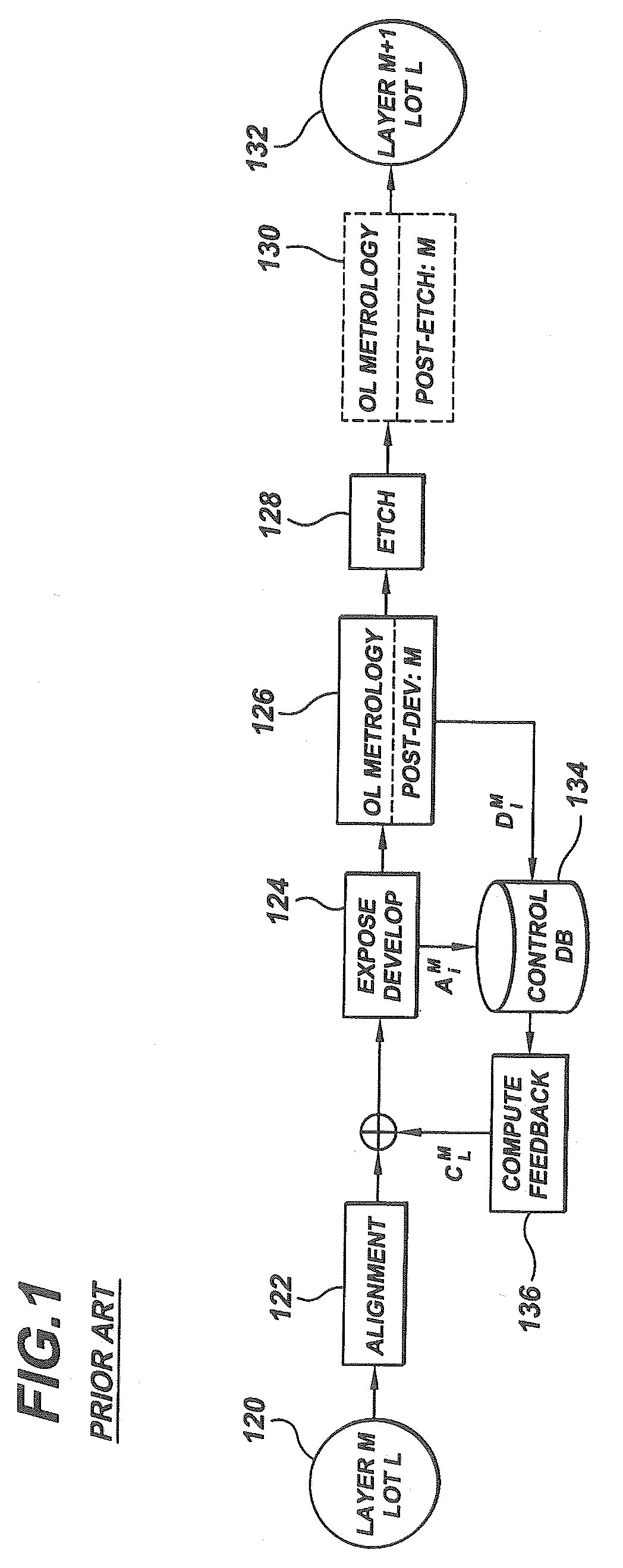
[0029]The present invention provides an improved method to permit the post etch measurement to be used to reduce the post lithography bias in the metrology. The method employs prior photo level, post etch measurement targets, which are usually visible at subsequent post lithography metrology steps. This enables the measurements for the level of interest to be compared to the post lithography measurements, so that error bias may be determined between the two. It has also been shown that this bias remains fairly constant for a given tool / process conditions.

[0030]The modeled error bias may be used by the APC application to correct the lithography control by adding the modeled bias to the last set of post lithography measurements. Although the bias may drift over time or after tool maintenance, i...


PUM


Abstract

A method of determining positioning error between lithographically produced integrated circuit patterns on at least two different lithographic levels of a semiconductor wafer comprising. The method includes exposing, developing and etching one or more lithographic levels to create one or more groups of marks comprising a target at one or more wafer locations. The method then includes exposing and developing a subsequent group of marks within the target on a subsequent lithographic level. The method then comprises measuring the position of the marks on each level with respect to a common reference point, and using the measured positions of the groups of marks to determine the relative positioning error between one or more pairs of the developed and etched lithographic levels on which the marks are located.

Description

BACKGROUND OF THE INVENTION[0001]1. Field of the Invention[0002]The present invention relates to the manufacture of integrated circuits and, in particular, to a method and system for determining overlay error in lithographic processing of integrated circuits.[0003]2. Description of Related Art[0004]Semiconductor manufacturing requires the sequential patterning of process layers on a single semiconductor wafer. Lithographic exposure tools known as steppers or scanners print multiple integrated circuit patterns or fields by lithographic methods on successive layers of the wafer. These exposure tools typically pattern different layers by applying step and repeat lithographic exposure or step and scan lithographic exposure in which the full area of the wafer is patterned by sequential exposure of the stepper fields containing one or more integrated circuits. Typically, 20-50 layers are required to create an integrated circuit.[0005]In order to match corresponding features in successive ...

Claims


Application Information

Patent Timeline
IPC IPC(8): G03F9/00
CPCG03F7/70633Y10S438/975
Inventor AUSSCHNITT, CHRISTOPHER P.MUTH, WILLIAM A.
Owner GLOBALFOUNDRIES INC
Why Eureka
Try Eureka