Method for producing bonded wafer

a technology of bonded wafers and active layers, applied in the direction of basic electric elements, electrical apparatus, semiconductor devices, etc., can solve the problems of poor thickness uniformity of active layers, inability to produce soi structures having different crystal orientations, and 30%, etc., to achieve good surface roughness, improve thickness uniformity, and reduce defects

Inactive Publication Date: 2009-07-23
SUMCO CORP
View PDF5 Cites 16 Cited by
  • Summary
  • Abstract
  • Description
  • Claims
  • Application Information

AI Technical Summary

Benefits of technology

[0020]According to the invention, there can be stably obtained the bonded wafer having not only the excellent thickness uniformity after the thinning but also good surface roughness and being much fewer in the occurrence of defects.

Problems solved by technology

Among the above methods, however, the grinding-polishing method has a problem that the thickness uniformity of the active layer is poor (±30% or more).
On the other hand, the method using oxygen ion implantation (SIMOX) has a problem that SOI structures having different crystal orientations can not be produced so as to interleave the insulating layer.

Method used


Image

  • Method for producing bonded wafer
  • Method for producing bonded wafer
  • Method for producing bonded wafer

Examples


example 1

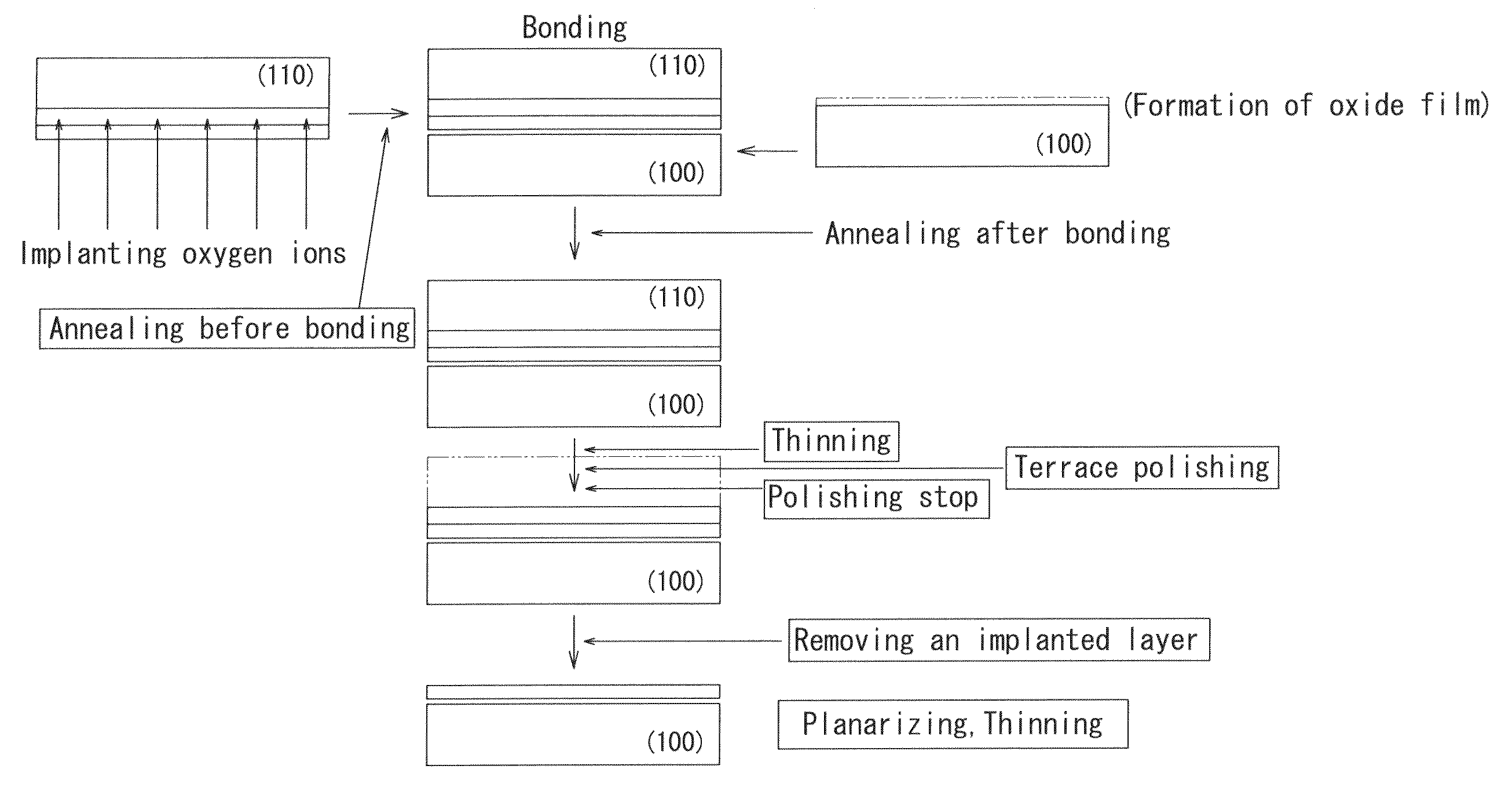
[0101]There are provided two silicon wafers of 300 mm in diameter sliced from a silicon ingot grown by CZ method and doped with boron. One of the two silicon wafers has a crystal orientation of (110) and is used as a wafer for active layer, and the other silicon wafer has a crystal orientation of (100) and is used as a wafer for support layer. Both the wafers are p-type silicon doped with boron and have a specific resistance of 1-20 Ωcm.

[0102]An oxide film having a thickness of 150 nm is formed on the (100) wafer by treating in an oxidizing atmosphere at 1000° C. for 5 hours.

[0103]Then, an oxygen ion implantation is carried out from the surface of the (110) wafer as the wafer for active layer at an acceleration voltage of 180 keV. The oxygen ion implantation is conducted at two stages, wherein the first ion implantation stage is carried out at a substrate-temperature of 200-600° C. and a dose is varied within a range of 1×10¹⁶−1×10¹⁸ atoms / cm2. In the second ion implantation stage, ...

example 2

[0113]A bonded wafer is prepared under the same conditions as in Example 1 except that the (110) wafer for active layer is bonded to the (100) wafer for support layer without an insulating film (an oxide film). The thus obtained active layer has a thickness of 100-200 nm and the scattering in the thickness distribution in the surface is within a range of 10-20%.

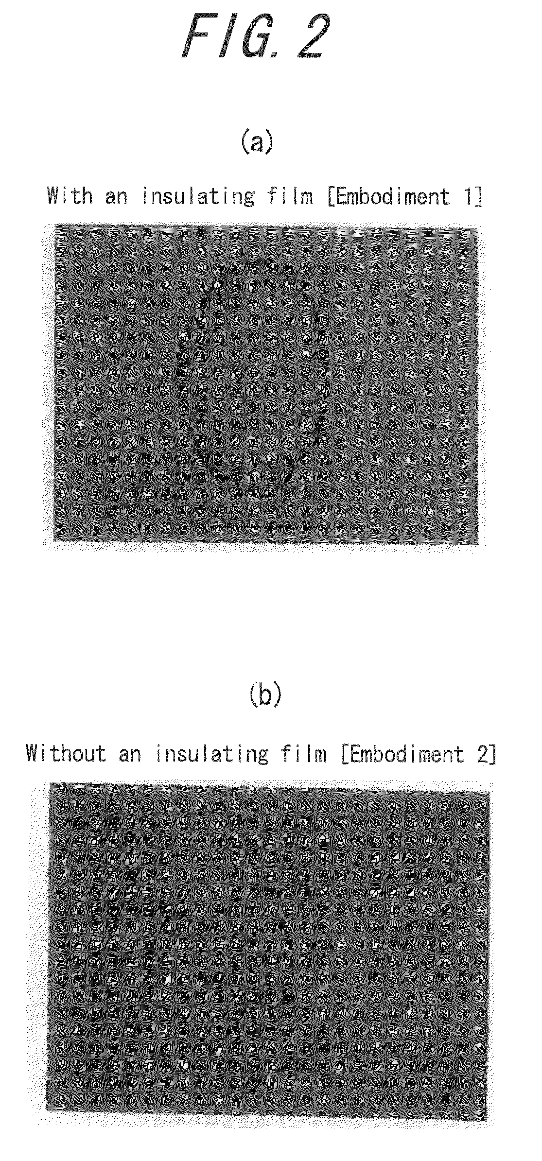
[0114]Next, the defect density of the bonded wafers obtained in Examples 1 and 2 is investigated.

[0115]The form of defects generated differs between Example 1 using the insulating film and Example 2 not using the insulating film.

[0116]FIGS. 2(a) and 2(b) show optical microphotographs of crystal defects generated on the wafer surfaces in Examples 1 and 2, respectively. When the bonding is carried out with the oxide film (Example 1), an ellipsoidally-shaped defect (diameter: 100-500 μm) is observed and also the oxide film is observed in such a defect. On the other hand, when the bonding is carried out without the oxide film (Ex...


PUM


Abstract

In the method for producing a bonded wafer by bonding a wafer for active layer to a wafer for support layer and then thinning the wafer for active layer, when oxygen ions are implanted into the wafer for active layer, the implantation step is divided into two stages conducted under specified conditions.

Description

BACKGROUND OF THE INVENTION[0001]1. Field of the Invention[0002]This invention is to effectively prevent deterioration of surface roughness and occurrence of defects particularly resulted from an oxygen ion implanted layer in the production of a bonded wafer.[0003]2. Description of the Related Art[0004]As a typical production method of a bonded wafer, there are known a method wherein a silicon wafer having an oxide film (insulating film) is bonded to another silicon wafer and then one side of the resulting bonded wafer is ground and polished to form SOI layer (grinding-polishing method), a method wherein oxygen ions are implanted into an interior of a silicon wafer and thereafter a high-temperature annealing is conducted to form a buried oxide film in the silicon wafer and then an upper portion of the oxide film is rendered into SOI layer (SIMOX), and a method wherein ions of hydrogen or the like are implanted into a surface layer portion of a silicon wafer for SOI layer (wafer for ...

Claims


Application Information

Patent Timeline
Patent Type & Authority Applications(United States)
IPC IPC(8): H01L21/30
CPCH01L21/26506H01L21/304H01L21/30608H01L2221/68363H01L21/6835H01L21/76243H01L21/76254H01L21/30625H01L27/12H01L21/265
Inventor MORIMOTO, NOBUYUKINISHIHATA, HIDEKIOKUDA, HIDEHIKOENDO, AKIHIKO
Owner SUMCO CORP
Why Eureka
Try Eureka