Heat transfer film, semiconductor device, and electronic apparatus

a technology of heat transfer film and semiconductor device, which is applied in the direction of electrical apparatus construction details, light and heating apparatus, natural mineral layered products, etc., can solve the problems of reducing the size of the device, difficult to cool a portable device with a small space, and difficult to transfer a sufficient amount of heat, etc., to achieve effective transfer of heat generated, small thickness, and high thermal conductivity

Active Publication Date: 2009-07-30
FURUKAWA ELECTRIC CO LTD
View PDF7 Cites 25 Cited by
  • Summary
  • Abstract
  • Description
  • Claims
  • Application Information

AI Technical Summary

Benefits of technology

[0050]In the present invention, it is possible to obtain the heat transfer layer with an extremely small thickness and an extremely high thermal conductivity in the in-plane direction thereof. Accordingly, it is possible to effectively transfer heat generated in the heating element such as the semiconductor device through the heat transfer layer. Therefore, it is possible to efficiently radiate and transfer heat generated in the heating element within a limited space.
[0051]In the present invention, it is possible to dissipate and diffuse a small amount of heat in a heat transfer process in the in-plane direction. Accordingly, it is possible to reduce a harmful effect on an electric device due to dissipation and diffusion of heat in the heat transfer process. Further, it is possible to cool the electronic apparatus and the semiconductor device used for such as an electronics field, a vehicle waste heat management field, or the like, in which it is necessary to efficiently transfer heat generated in the semiconductor device or the like. Still further, it is possible to cool a portable device in a limited space.
[0052]In the present invention, it is possible to efficiently radiate and transport heat generated in a limited space through the heat transfer layer. Accordingly, it is possible to provide the semiconductor device with a small size capable of efficiently radiating transporting heat. Further, it is possible to cool a portable device such as a portable telephone or the like.

Problems solved by technology

Accordingly, it is difficult to reduce a size of a device with the heat transfer module, thereby making it difficult to cool a portable device with a small space.
Accordingly, it is difficult to transfer a sufficient amount of heat.
Further, heat tends to dissipate or diffuse in the heat transfer process, thereby causing a harmful effect on the device.
Accordingly, it is difficult to substantially improve the thermal conductivity.

Method used


Image

  • Heat transfer film, semiconductor device, and electronic apparatus
  • Heat transfer film, semiconductor device, and electronic apparatus
  • Heat transfer film, semiconductor device, and electronic apparatus

Examples


first embodiment

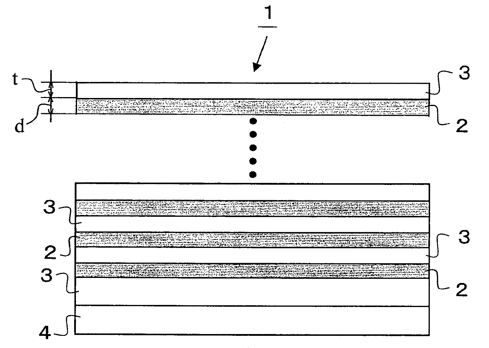
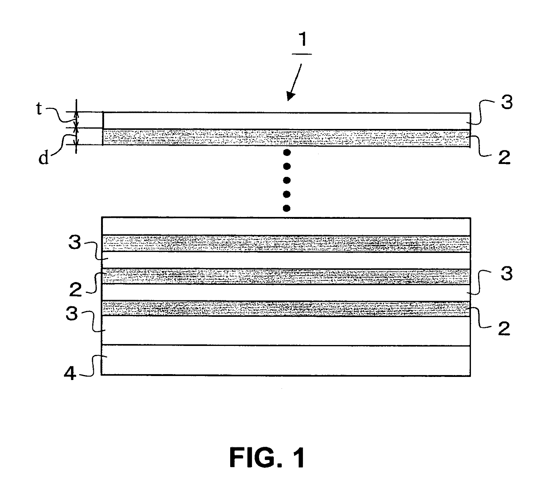
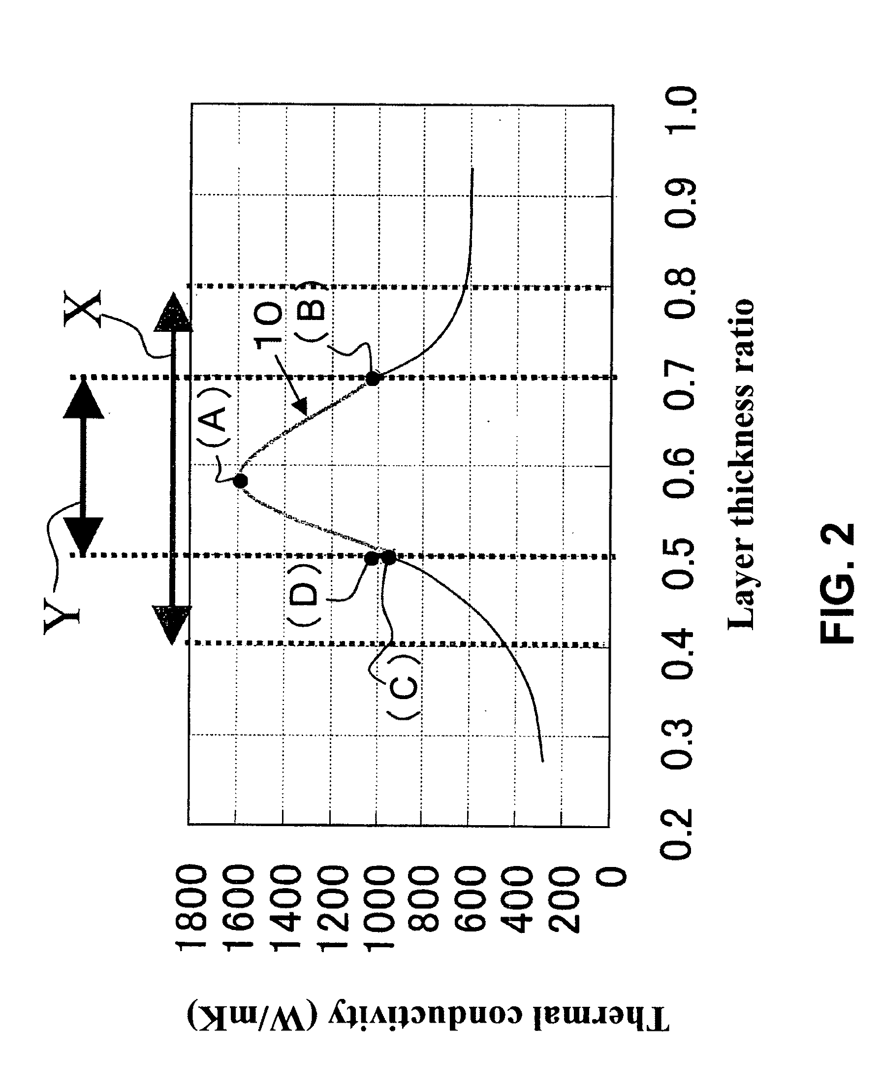
[0072]A first embodiment of the present invention will be described in detail below, based on FIG. 1 to FIG. 5. FIG. 1 is a cross sectional view showing a heat transfer layer according to the first embodiment, FIG. 2 is a graph showing a relation between a layer thickness ratio and a thermal conductivity in in-plane direction, FIG. 3 is a partially enlarged graph of FIG. 2, and FIGS. 4(A) to 4(D) are views showing a mechanism of a heat transfer enhancement by optimizing a configuration of a layer thickness.

[0073]A heat transfer layer 1 as shown in FIG. 1 is configured by stacking a heat transfer layer 2 comprised of a first constituent material as a material including C (carbon) for transferring heat in in-plane direction and a layer thickness direction, and a strain relaxation layer 3 comprised of a second constituent material for relaxing a strain of the first constituent material. Here, a symbol 4 designates a silicon (Si) substrate.

[0074]According to the heat transfer layer 1, a...

second embodiment

[0122]FIG. 5 is a cross sectional view showing a configuration of a semiconductor device according to the second embodiment of the present invention, and FIG. 6 is a cross sectional view showing a configuration of a conventional semiconductor device as a comparative example. Here, a duplicated description is omitted with using a similar symbol for the similar component part regarding FIG. 5 and FIG. 6.

[0123]According to the semiconductor device as shown in FIG. 5, the heat transfer layer 1 as shown in FIG. 1 is formed in the most vicinity of an active layer 21 in an LED (a light emitting diode) chip 20 as a semiconductor light emitting element. More specifically, the heat transfer layer 1 is provided at a peripheral part of a light transmission part 22 existing in the most vicinity of the active layer 21 in the LED chip 20.

[0124]Light emitted from the active layer 21 of the LED chip 20 is transmitted through the light transmission part 22 and then output outward. Here, the silicon s...

third embodiment

[0129]FIG. 7 is a cross sectional view showing a configuration of a semiconductor device according to the third embodiment of the present invention, and FIG. 8 is a cross sectional view showing a configuration of a conventional semiconductor device as a comparative example. Here, a duplicated description is omitted with using a similar symbol for the similar component part regarding FIG. 7 and FIG. 8.

[0130]The semiconductor device as shown in FIG. 7 is configured as a communications laser module, and FIG. 7 shows a part of the communications laser module. In a semiconductor laser diode 30 as a semiconductor light emitting element, the heat transfer layer 1 as shown in FIG. 1 is formed. More specifically, the heat transfer layer 1 is formed in the vicinity of an active layer 31 in the semiconductor laser diode 30 inside. Moreover, a symbol 32 designates an edge face at a light output side regarding edge faces of a resonator, and light generated in the active layer 31 is output from t...


PUM

PropertyMeasurementUnit
thicknessaaaaaaaaaa
thicknessaaaaaaaaaa
thicknessaaaaaaaaaa

Abstract

A heat transfer film includes a heat transfer layer formed of a first constituent material containing C (carbon) for transferring heat in an in-plane direction thereof and a layer thickness direction thereof; and a strain relaxation layer formed of a second constituent material and laminated on the heat transfer layer for relaxing a strain in the heat transfer layer. The first constituent material includes a graphite, and the second constituent material includes an amorphous material.

Description

BACKGROUND OF THE INVENTION AND RELATED ART STATEMENT[0001]The present invention relates to a heat transfer film, a semiconductor device, and an electronic apparatus comprising the heat transfer film. The heat transfer film, the semiconductor device, and the electronic apparatus are used in an electronics field and a vehicle waste heat management field, in which it is necessary to efficiently transfer heat generated in the electronic apparatus and the semiconductor device.[0002]Conventionally, in a case of radiating or transporting heat generated by a semiconductor device, such as an electronic apparatus, an electronic device, an optical device, or the like, heat transport is performed through heat exchange with a liquid or transferring heat to a material with a high thermal conductivity. For example, a single layer is formed of a graphite material as a heat conducting material.[0003]Patent Reference has disclosed an anisotropic heat conducting material comprised of a combination of...

Claims


Application Information

Patent Timeline
Patent Type & Authority Applications(United States)
IPC IPC(8): H05K7/20B32B7/02
CPCH01L21/268H01L21/84H01L23/373H01L23/3735Y10T428/30H01L2924/0002H01L33/641H01L2924/00
Inventor KATAYAMA, MASAKOFUJIWARA, HIDEMICHI
Owner FURUKAWA ELECTRIC CO LTD
Why Eureka
Try Eureka