Crystallizing method, thin-film transistor manufacturing method, thin-film transistor, and display device

a technology of thin film transistors and manufacturing methods, applied in the direction of manufacturing tools, instruments, transportation and packaging, etc., can solve the problems of difficult use of xecl lasers, inability to meet the requirements of low-temperature treatment, and poor mobility of mos transistors fabricated by using silicon single crystals, etc., to reduce the occurrence of crystallization displacement, and save electricity

Inactive Publication Date: 2009-08-06
SHARP KK
View PDF16 Cites 32 Cited by
  • Summary
  • Abstract
  • Description
  • Claims
  • Application Information

AI Technical Summary

Benefits of technology

[0014]It is, accordingly, an object of the present invention to provide a crystallizing method capable of realizing crystallization with a large grain size even at room temperature, achieving electric power saving, and reducing the occurrence of the displacement of crystallization, a thin-film transistor manufacturing method, a thin-film transistor, and a display device.
[0015]According to an aspect of the present invention, use of a laser beam with wavelength of the lowest light absorption possible in a crystallizing optical system prevents the optical system from generating heat and reduces the occurrence of the displacement of crystallization. The present invention provides a crystallizing method of achieving crystallization with a large grain size at relatively low electric power by providing at least one SiOx film (x is less than 2) on the laser beam incident face of a non-single-crystal semiconductor film and causing a part of the crystallizing laser beam to be absorbed. The present invention further provides a thin-film transistor manufacturing method, a thin-film transistor, and a display device.
[0022]According to still another aspect of the present invention, there is provided a thin-film transistor manufacturing method comprising a step of forming at least one layer of SiOx film (x is less than 2) on the laser beam incident face of a non-single-crystal semiconductor film provided on a substrate; a step of irradiating a homogenized pulse laser beam whose wavelength is 248 nm or 300 nm or more onto the non-single-crystal semiconductor film via the SiOx film, allowing the SiOx film not only to absorb a part of the pulse laser beam and generate heat but also to melt the irradiated part of the non-single-crystal semiconductor film, and forming a crystallization region in the non-single-crystal semiconductor film after the pulse laser beam is cut off; and a step of forming a thin-film transistor aligned with the crystallization region.
[0030]According to aspect of the present invention, it is possible to provide a crystallizing method capable of realizing crystallization with a large grain diameter even at room temperature, achieving electric power saving, and reducing the occurrence of the displacement of crystallization, a thin-film transistor manufacturing method, a substrate to be crystallized, a thin-film transistor, and a display device.

Problems solved by technology

This mobility is much inferior to that of a MOS transistor fabricated by using a silicon single crystal.
Thus, it can be used for KrF laser whose wavelength is 248 nm among excimer lasers, but is difficult to use for XeCl laser now often used in mass production whose wavelength is 308 nm, because it becomes transparent.
Furthermore, in the methods in the document by W. Yeh and M. Matsumura and the document by M. Hiramatsu, et al., the substrate has to be heated to a high-temperature region to make crystal grains larger in its size, preventing the requirement for low-temperature treatment from being met, which is a problem.
Since the substrate heating temperature may exceed, for example, 500 degrees, general-purpose glass (e.g., soda glass) or plastic is liable to deteriorate or deform due to heating.
Furthermore, since heating the substrate 103 increases the power consumption, electric power saving particularly required in industrialization is not satisfied.
In the heat generation, the temperature rises with time, which results in the blurring of the focal point of the lens and the displacement of the crystallization position.
When a transistor circuit is formed, the channel region is formed off the crystallization region in the exposure process, with the result that the yield becomes worse in the mass production process.
Furthermore, in a display device, it is understood that display irregularity and color nonuniformity occur, which causes poor display.

Method used


Image

  • Crystallizing method, thin-film transistor manufacturing method, thin-film transistor, and display device
  • Crystallizing method, thin-film transistor manufacturing method, thin-film transistor, and display device
  • Crystallizing method, thin-film transistor manufacturing method, thin-film transistor, and display device

Examples


Embodiment Construction

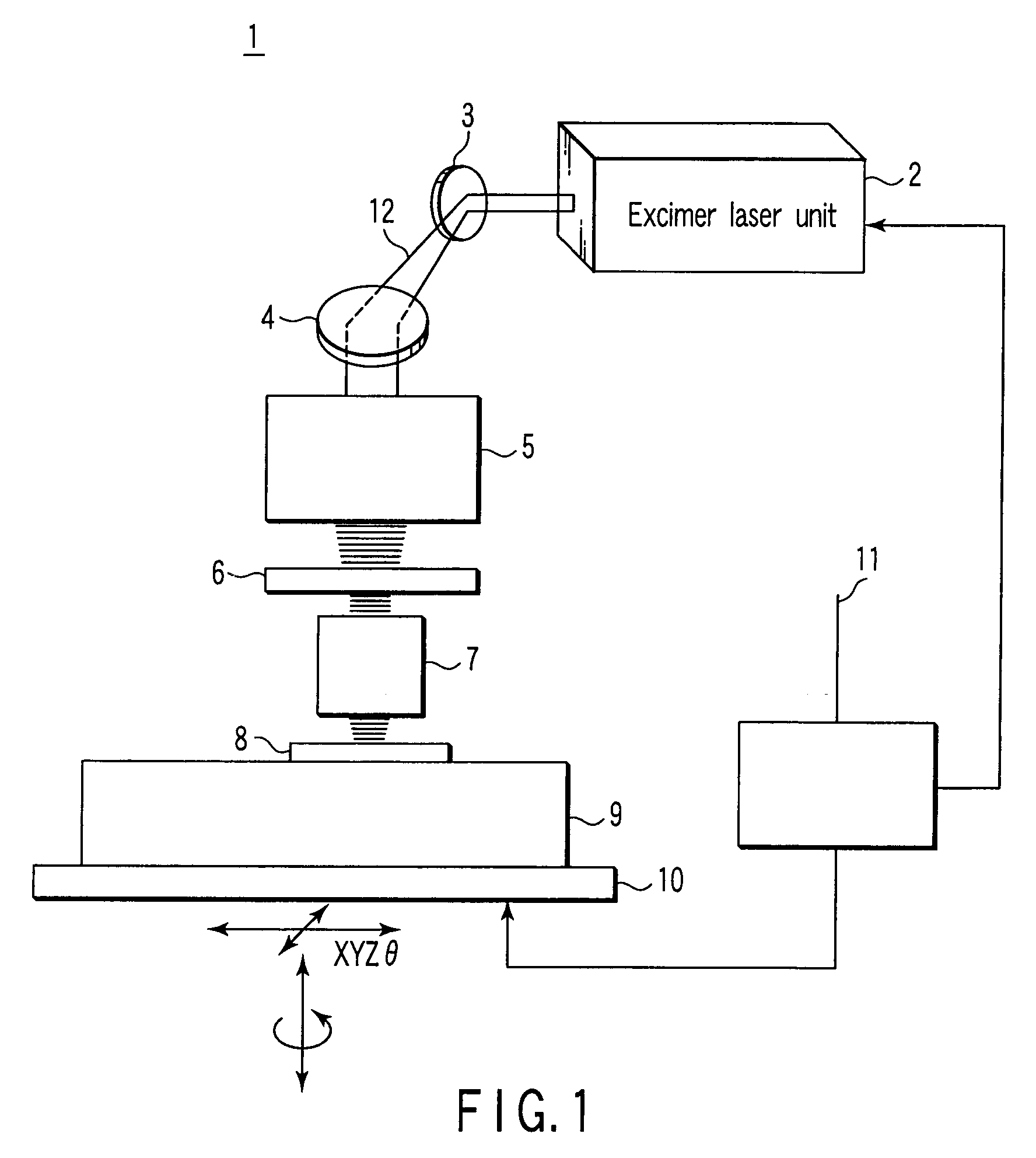
[0050]Hereinafter, referring to the accompanying drawings, a preferred embodiment of the present invention will be explained.

[0051]First, the technical terms used in this specification are defined as follows. “Lateral growth” means that, when a film to be crystallized is melted and solidified, the growth of a crystal grain progresses laterally along the film surface. “Input fluence” is a measure representing the energy density of a laser beam for crystallization. It is obtained by integrating the amount of one shot pulse laser beam energy per unit area. Specifically, it means the average light intensity of a laser beam measured at a light source or in the irradiation region (irradiation field).

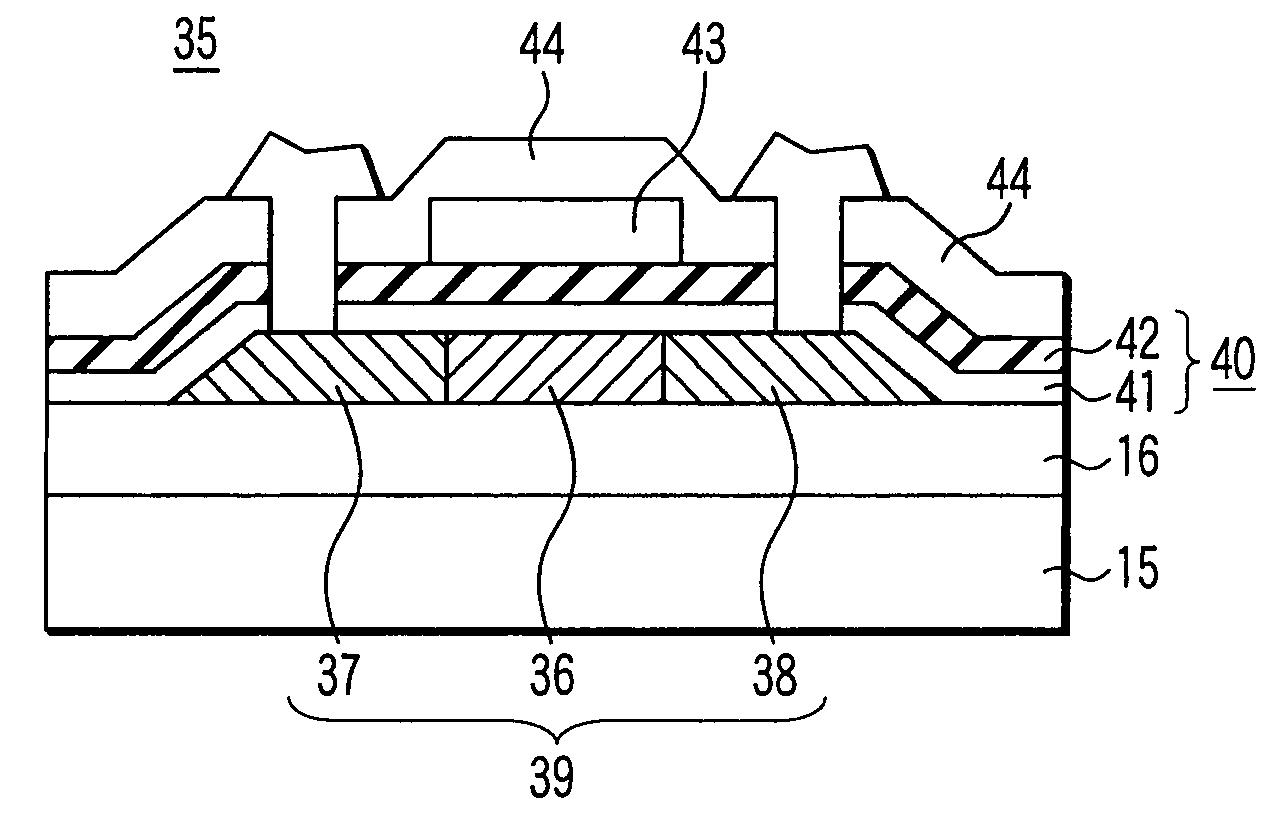
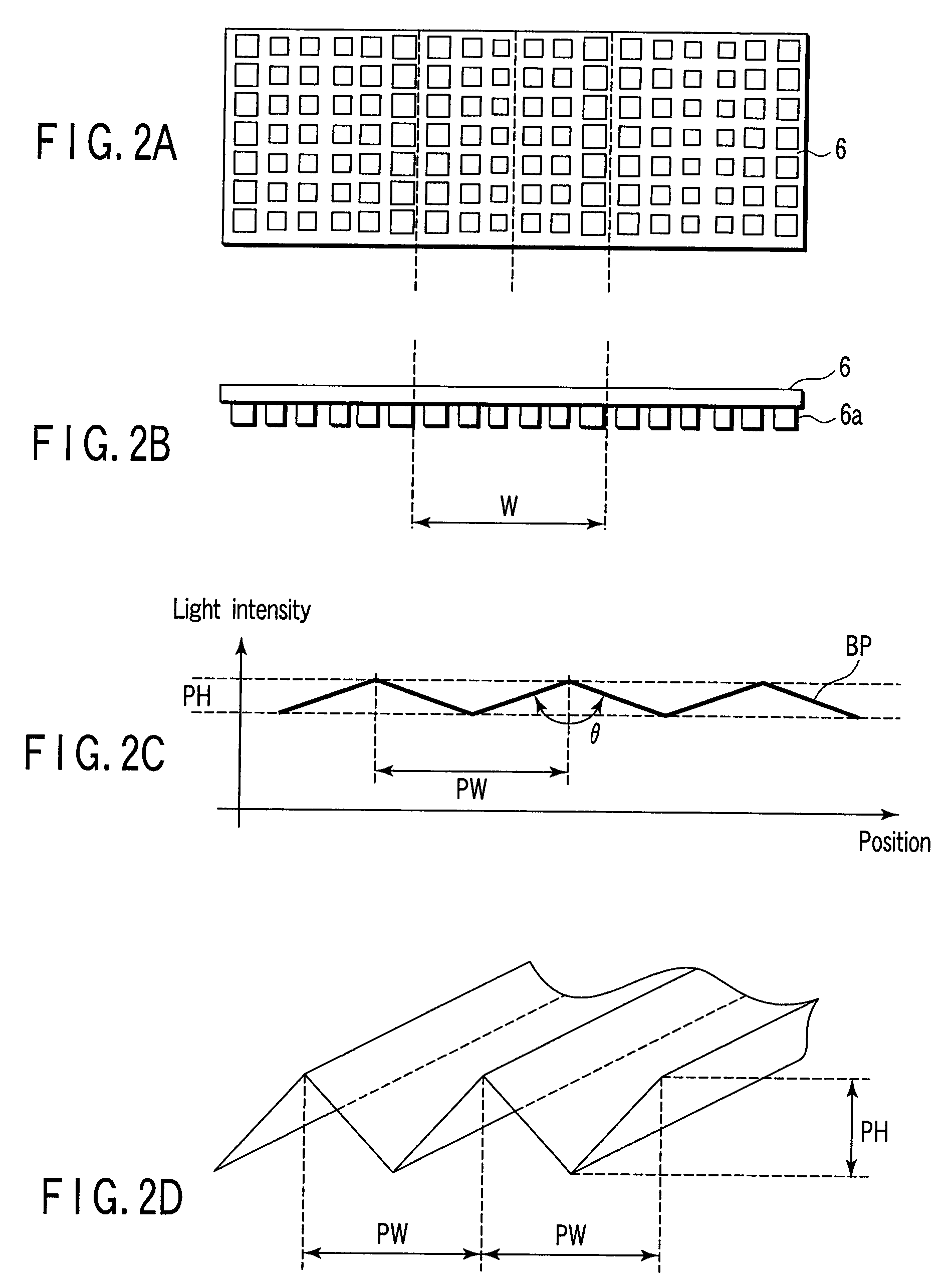
[0052]“Phase shifter” is an example of a phase modulation optical system. It is a spatial intensity modulation optical element for modulating the phase of the laser beam and is distinguished from a phase shift mask used in the exposure step in the photolithographic process. For example, a phas...


PUM

PropertyMeasurementUnit
grain sizeaaaaaaaaaa
wavelengthaaaaaaaaaa
bandgap energyaaaaaaaaaa

Abstract

A crystallizing method of causing a phase shifter to phase-modulate a laser beam whose wavelength is 248 nm or 300 nm or more from an excimer laser unit into a laser beam with a light intensity profile having a plurality of inverted triangular peak patterns in cross section and of irradiating the pulse laser beam onto a substrate to be crystallized for crystallization. The substrate to be crystallized is such that one or more silicon oxide films which present absorption properties to the laser beam and differ in the relative proportions of Si and O are provided on a laser beam incident face.

Description

CROSS-REFERENCE TO RELATED APPLICATIONS[0001]This application is a divisional of application Ser. No. 11 / 136,371 filed May 25, 2005 which is based upon and claims the benefit of priority from prior Japanese Patent Applications No. 2004-196111, filed Jun. 4, 2004; No. 2004-254283, filed Sep. 1, 2004; No. 2004-286646, filed Sep. 30, 2004; and No. 2005-076190, filed Mar. 17, 2005, the entire contents of all of which are incorporated herein by reference.BACKGROUND OF THE INVENTION[0002]1. Field of the Invention[0003]This invention relates to a crystallizing method suitable for use in a display device, such as a liquid crystal or organic electroluminescence (EL), a thin-film transistor manufacturing method, a thin-film transistor, and a display device.[0004]2. Description of the Related Art[0005]The driving circuit for a display device, such as a liquid-crystal display device, has been fabricated by using an amorphous semiconductor film formed on a glass substrate. With the expansion of ...

Claims


Application Information

Patent Timeline
Patent Type & Authority Applications(United States)
IPC IPC(8): H01L29/786H01L21/268B32B7/00H01L21/336B23K26/06H01L21/00H01L21/20H01L21/26H01L21/324H01L21/42H01L21/477H01L21/77H01L21/84
CPCB23K26/0656H01L21/2026H01L21/268Y10T428/265H01L29/66757H01L27/1296H01L27/1285B23K26/066H01L21/02425H01L21/02686H01L21/02678H01L21/02488H01L21/02422H01L21/02532H01L21/0242H01L21/02595H01L21/02381H01L21/02691H01L29/78675H01L21/0268
Inventor HIRAMATSU, MASATOOGAWA, HIROYUKIMATSUMURA, MASAKIYO
Owner SHARP KK
Why Eureka
Try Eureka