Signal transmission system and semiconductor integrated circuit device

a transmission system and integrated circuit technology, applied in the direction of near-field systems using receivers, semiconductor/solid-state device details, pulse techniques, etc., can solve the problems of reducing the number of wires, the inability to stack semiconductor chips of the same shape, and the microfabrication of transistor elements approaching its limit, etc., to achieve thin semiconductor substrates, increase power consumption, and a large coil size

Active Publication Date: 2009-08-06
NEC CORP
View PDF2 Cites 24 Cited by
  • Summary
  • Abstract
  • Description
  • Claims
  • Application Information

AI Technical Summary

Benefits of technology

[0056]In accordance with the present invention, data can be transmitted at a high S / N ratio without occurrence of problems of increased power consumption, enlarged coil size and thinned semiconductor substrate. Accordingly, a signal transmission system using inductive coupling capable of reducing malfunction due to noise is obtained, as well as a semiconductor integrated circuit device that uses this system.

Problems solved by technology

However, functions and memory capacity that exceed even the increases in multiple functions and memory capacity obtained by microfabrication of transistor elements are sought in recent semiconductor integrated circuit devices, and the microfabrication of transistor elements is approaching its limit.
In order to assure pad area (e.g., 100 μm square), therefore, a problem which arises is that a limitation is imposed upon the number of wires.
Consequently, a problem which arises is that semiconductor chips of the same shape cannot be stacked.
This is a factor that limits an improvement in performance.
A problem which arises is that the process for manufacturing the semiconductor integrated circuit device is complicated, thereby raising manufacturing cost and prolonging manufacturing time.
This means that the number of layers of stacked semiconductor chips is limited to two, and it is difficult to stack the chips in three or more layers.
A problem which arises is that a limitation is imposed upon an increase in number of functions and enlargement of memory capacity.
Consequently, if current is passed through the transmitting coil 100 when there is no change in the transmit data, power is consumed wastefully.
However, the conventional signal transmission system is one in which data is sent and received using a transmitting coil and a receiving coil only at the timing at which transmit data changes, as illustrated in FIG. 13, Consequently, in a case where transmit data of successive “1”s or “0”s is transmitted, there is a higher possibility that the receiving circuit will malfunction owing to noise.
Examples of noise that enter the receiving circuit are disturbance noise that enters from outside the semiconductor integrated circuit device, noise that enters the transmitting coil from a logic circuit or transmitting circuit mounted on the semiconductor chip on the data-transmit side, and noise that enters the receiving coil from a logic circuit or receiving circuit mounted on the semiconductor chip on the data-receive side.
Since the timing at which noise enters the receiving coil is uncertain, however, it is not possible to predict the timing at which noise will enter and to control the time of the rising edge of the receive signal so as not to coincide with this timing.
Accordingly, malfunction due to noise cannot be prevented with a method of optimally setting or controlling transmission and reception timings of the receive clock.
However, since the polarity of the noise and the polarity of the transmit data usually are independent of each other, malfunction due to noise cannot be prevented.
However, with the method of increasing the induced voltage of the receiving coil by increasing a current that flows into the transmitting coil, it is difficult to accurately ascertain the magnitude of noise that enters the receiving coil.
Consequently, the induced voltage produced by the receiving coil is mnade larger than necessary and power is consumed wastefully by the semiconductor integrated circuit device,
Consequently, the strength of the semiconductor chips declines, destruction occurs more easily at the time of manufacture of the semiconductor integrated circuit device and this is a cause of diminished product yield.
However, since it is difficult to accurately ascertain the magnitude of noise that enters the receiving coil, as mentioned above, it is difficult to set the threshold-value voltage optimally.
As a result, the problems of increased power consumption, enlarged coil size and thinned semiconductor substrate do not arise.

Method used


Image

  • Signal transmission system and semiconductor integrated circuit device
  • Signal transmission system and semiconductor integrated circuit device
  • Signal transmission system and semiconductor integrated circuit device

Examples


Embodiment Construction

[0095]Next, the present invention will be described with reference to the drawings.

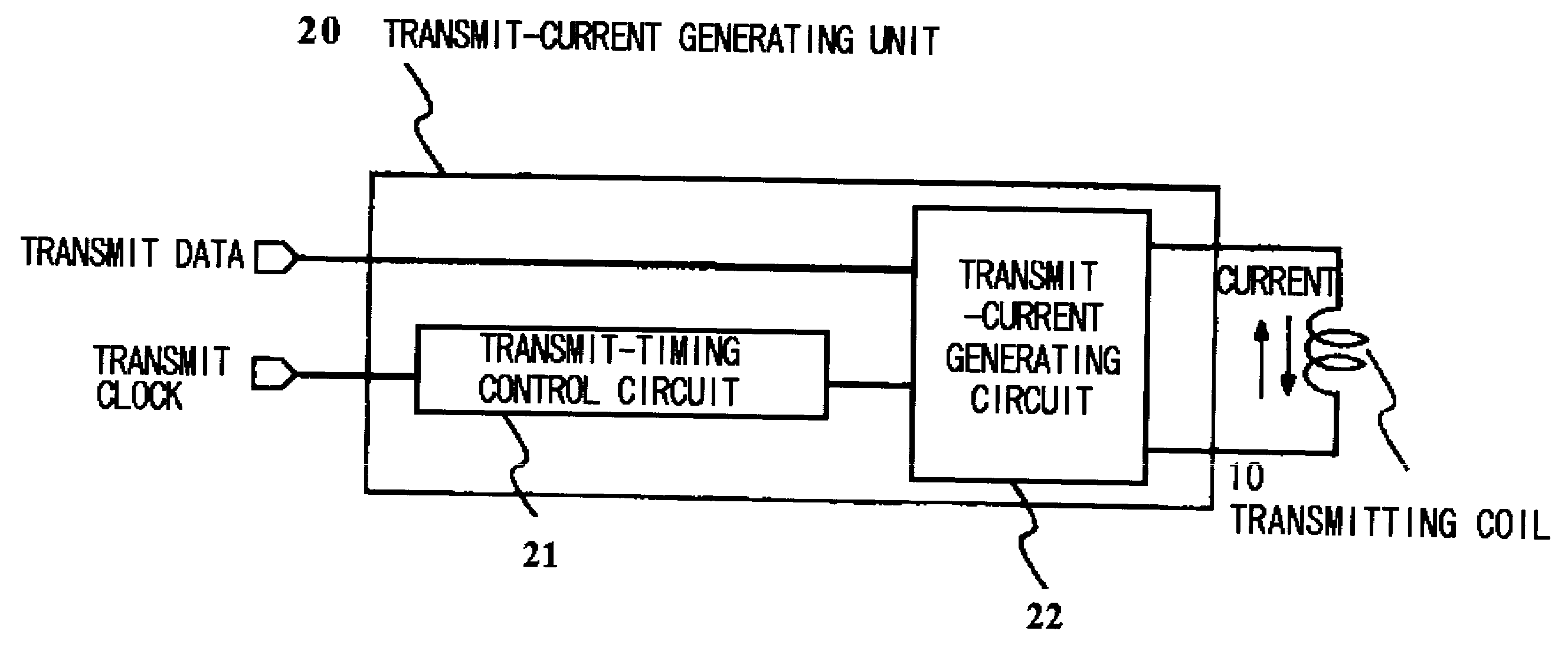
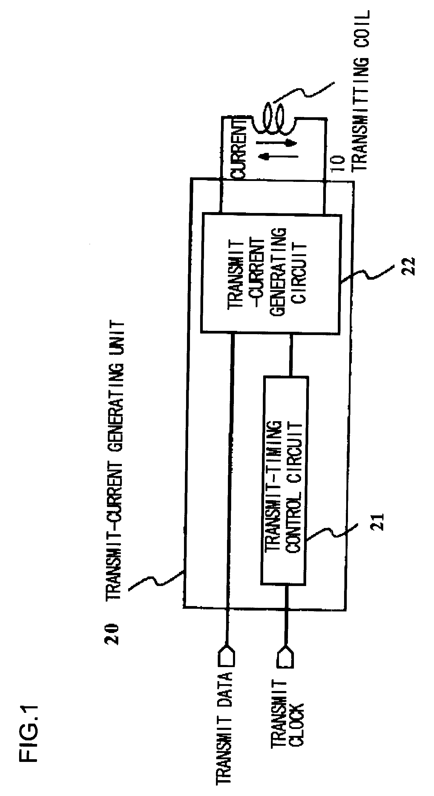
[0096]FIG. 1 is a block diagram illustrating an example of the configuration of a transmitting circuit used by a signal transmission system according to the present invention.

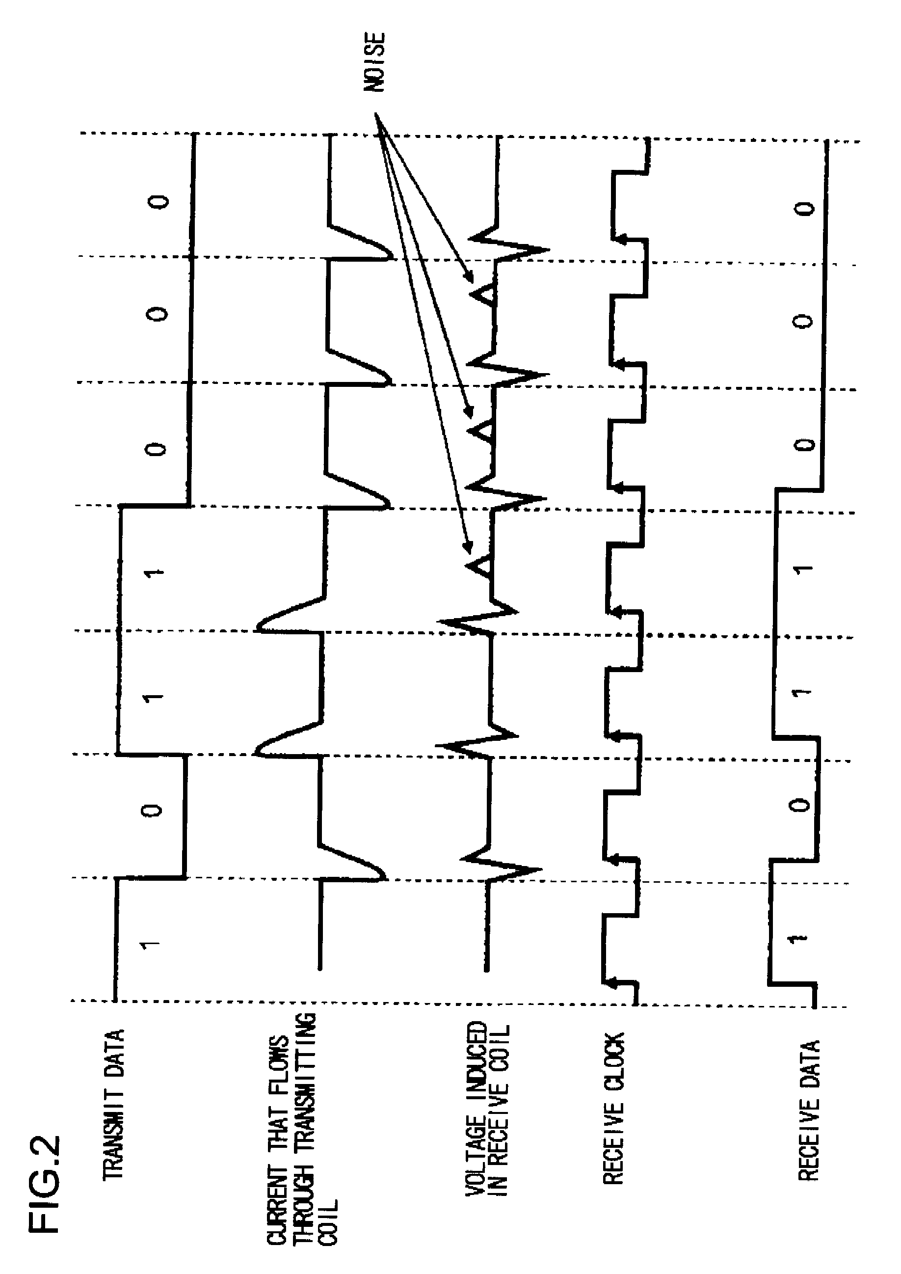
[0097]As illustrated in FIG. 1, the transmitting circuit used by the signal transmission system of the present invention includes a transmitting coil 10 and a transmit-current generating unit 20 for supplying a current through the transmitting coil 10 at every rising edge or falling edge of a clock used in transmission of data. Transmit data and a clock (transmit clock) used in data transmission are supplied to the transmit-current generating unit 20.

[0098]The transmit-current generating unit 20 has the transmit-timing control circuit 21 and the transmit-current generating circuit 22. The transmit-timing control circuit 21 generates a timing signal that decides the timing at which current is passed through the transmitting coil 1...


PUM


Abstract

Disclosed is a semiconductor integrated circuit device including a transmitting circuit and a receiving coil inductively coupled to a transmitting coil. The transmitting circuit transmits data by supplying a current through the transmitting coil not at the time of transition of data but at every rising edge or falling edge of a clock used in transmission of data. At every rising edge or falling edge of the clock, a receiving circuit captures a voltage induced in the receiving coil due to the current flowing through the transmitting coil, reproduces the transmitted data and outputs the reproduced data.

Description

TECHNICAL FIELD[0001]This invention relates to a signal transmission system for transmitting data among a plurality of semiconductor chips and to a semiconductor integrated circuit device equipped with this system.BACKGROUND ART[0002]The integration density of semiconductor integrated circuit devices has been improved with the microfabrication of transistor elements and these devices are now capable of implementing multiple functions with a single semiconductor chip. Further, the microfabrication of transistor elements has been accompanied by progress in increasing the storage capacity of semiconductor memories, regardless of the type thereof, such as a DRAM (Dynamic Random-Access Memory) or SRAM (Static Random-Access Memory).[0003]However, functions and memory capacity that exceed even the increases in multiple functions and memory capacity obtained by microfabrication of transistor elements are sought in recent semiconductor integrated circuit devices, and the microfabrication of ...

Claims


Application Information

Patent Timeline
Patent Type & Authority Applications(United States)
IPC IPC(8): H04L7/02H04B5/00
CPCH01L23/48H04B5/02H01L2924/0002H01L2924/00
Inventor FUKAISHI, MUNEONAKAGAWA, YOSHIHIROKURODA, TADAHIRO
Owner NEC CORP
Why Eureka
Try Eureka