Semiconductor and method for producing the same

a technology of semiconductors and semiconductors, applied in the direction of semiconductor devices, electrical devices, transistors, etc., can solve the problems of difficult -doping using a plurality of elements as dopants by solid phase epitaxy, and the difficulty of achieving the -doping technique itself, and achieve the effect of suppressing the segregation of doping on the surfa

Inactive Publication Date: 2009-08-13
NAT INST FOR MATERIALS SCI
View PDF2 Cites 6 Cited by
  • Summary
  • Abstract
  • Description
  • Claims
  • Application Information

AI Technical Summary

Benefits of technology

[0034]As described above according to the present invention, superimposed doping can be applied to an elemental semiconductor substrate such as of silicon which was difficult so far and, further, a semiconductor having a doping layer at high concentration can be attained.
[0035]More specifically, according to the invention, superimposed doping of a plurality of dopants can be attained while suppressing surface segregation of doping in the elemental semiconductor such as silicon, with no use of expensive apparatus such as an ion implantation apparatus and with no requirement for extra processing time by using a usual crystal growing apparatus. Further, superimposed doping is possible, in principle, at the level of an atomic layer and deviation of the concentration distribution for a plurality of superimposed dopants can be decreased substantially to zero in principle.
[0036]Accordingly, it is possible to restrict the concentration distribution width of a plural of dopants at least to 20 nm or less and the deviation for the concentration distribution of the plurality of superimposed dopants within 2 nm which were considered impossible so far.
[0037]Further, since such stable superimposed dopant is possible, a superimposed doping layer of a plurality of element dopants having a profile width at the order of an atomic layer can be formed in an elemental semiconductor according to the present invention.
[0038]This extends the range of application as the process in view of the manufacture of the semiconductor device.
[0039](1) In a case of using a doping layer as a simple conduction carrier (electron or hole) generation source, a superimposed doping layer where a plurality of dopants generating compression strain and expansion strain to the lattice constant of an elemental semiconductor are present together can be attained and a semiconductor device having a doping layer at high concentration can be provided.

Problems solved by technology

While it is intended to utilize the δ-doping technique of conducting superimposed doping of a plurality of dopants also in an elemental semiconductor such as silicon, the attainment of the δ-doping technique itself is difficult different from the compound semiconductor.
This is because δ-doping using a plurality of elements as dopants by solid phase epitaxy was difficult so far in the elemental semiconductor.
As a significant problem, it can not be said that the solid phase epitaxy is an ideal method as a technique of conducting doping to a predetermined depth.
The problem in the δ-doping technique is that a doping profile prevails in silicon solid phase epitaxy during solid phase epitaxy.
Further, the process requires much labor and long time.
Accordingly, it may be considered that control for the concentration and the distribution width is extremely difficult in the multi-element δ-doping technique that utilizes the solid phase epitaxy.
However, also the ion implantation technique is not ideal as a technique of doping to a predetermined depth.
Primarily, in the ion implantation technique, the apparatus is expensive and the implantation depth and the doping profile are determined depending on the acceleration energy of implanted ions and the mass of the ions and, further, annealing is necessary for repairing lattice damages caused upon implantation.
Theoretically, while superimposed doping for a plurality of dopants of implanting a plurality of elements into a substantially predetermined depth is possible, the distribution width can not be made identical.
Further, in the technique intending to determine the doping position at a nanometer scale as in the δ-doping technique, error for positioning is not possible at the order of nanometer, and deviation of the depth is fetal.

Method used


Image

  • Semiconductor and method for producing the same
  • Semiconductor and method for producing the same
  • Semiconductor and method for producing the same

Examples


example 1

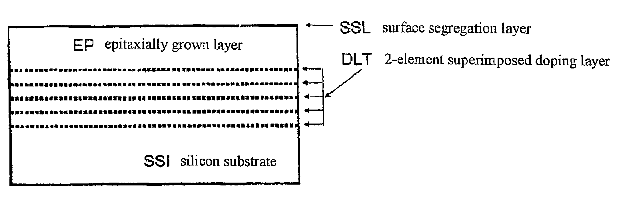
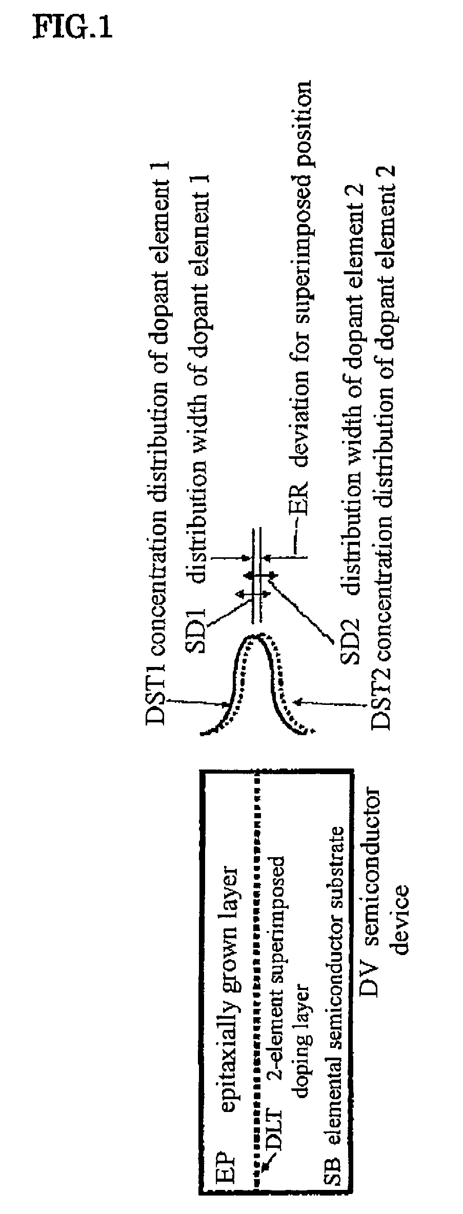
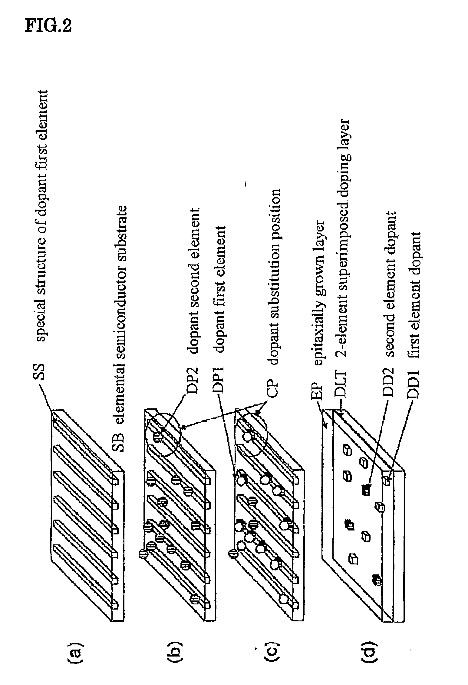
[0053]Description is to be made to a first example referring to FIG. 1 and FIG. 2. This example can include a silicon (001) crystal substrate as an elemental semiconductor substrate SB, a bismuth element as a first dopant element DP1, a bismuth thin line structure as a special surface structure SS of the first dopant element DP1, and an erbium element as the second dopant element DP2.

[0054]FIG. 3 shows the processing procedures of this example. Bismuth is vapor deposited at a substrate temperature T1 over a silicon (001) substrate to form the bismuth thin line structure. T1 is selected within a range of a temperature (500° C. to 600° C.) near the evaporation temperature of bismuth from above the silicon substrate. The time for forming the bismuth thin line structure is different depending on the temperature but there is no other differences. Successively, the temperature of the substrate is lowered to T2 to conduct deposition of erbium and deposition of silicon. In the case of this ...

example 2

[0072]Description is to be made for another example with reference to FIG. 1 and FIG. 2. This example can include a silicon (001) crystal substrate as an elemental semiconductor substrate SB, a bismuth element as a first dopant element DP1, a bismuth thin line structure as a special surface structure SS of the first dopant DP1, and an antimony element as a second dopant element DP2. The vapor deposition of antimony was conducted also at a substrate temperature T1 of 400° C. as in Example 1, and the total vapor deposition amount of antimony was defined as a 1-atomic layer. A report investigating the concentration distribution of the bismuth element and the antimony element in the state corresponding to FIG. 2(c) is described in the document: Bismuth and Antimony Nanoline in Si Epitaxial Layer. Microscopy of Semiconducting Materials 1999 (Edited by A G Cullis, and J. L. Hutchison, IOP Publishing Ltd., London), Inst. Phys. Conf. Ser. vol. 164 (1999), pp 167-170, K. Miki, H. Matsuhata, ...

example 3

[0073]Other example is shown in FIG. 13. The constitution is different from the examples described above in that the superimposed doping layer is formed repetitively. This is an effective means in a case of attaining a desired amount by repetition when the dopant amount of the superimposed doping layer is insufficient when applied for once, or intending to obtain doping at a certain concentration over a considerable thickness. The cross sectional shape of the obtained doping structure is shown in FIG. 12.

[0074]This example has one important feature as the doping technique. That is, the repetition of a plurality of doping can be simply realized by merely changing the substrate temperature and controlling the vapor deposition amount in this patent. This contrasts to the δ-doping method and the ion implantation technique as the prior method, which require serious procedures even for conducting doping only by once. Control can be attained by using those described in the example with ref...


PUM


Abstract

A method for producing a semiconductor by conducting superimposed doping of a plurality of dopants in a semiconductor substrate, which includes evaporating a (2×n) structure by a first dopant and forming its thin line structure on the substrate, then bringing the semiconductor substrate to a temperature capable of epitaxial growth, vapor depositing a second or third or subsequent dopants above the semiconductor substrate where the first dopant has been deposited, then epitaxially growing a semiconductor crystal layer over the semiconductor substrate, subsequently forming a superimposed doping layer composed of the first, second, or the third or subsequent dopants in the semiconductor substrate, and applying an annealing treatment to the superimposed doping layer at a high temperature, thereby activating the plurality of dopants electrically or optically. Superimposed doping of a plurality kinds of elements as dopants can thus be performed to a predetermined depth also in the case of an elemental semiconductor.

Description

TECHNICAL FIELD[0001]The present invention relates to a semiconductor having a superimposed doping layer of a plurality of element dopants and a method for producing the same.BACKGROUND ART[0002]A doping technique for a semiconductor device is essential as a process for manufacturing a semiconductor device. As a method of doping, a δ-doping technique has been known which is used as an effective method for improving the operation speed of a high mobility transistor. The method is based on that provision of a doping layer at the level of an atomic layer near the hetero interface enables to inject carriers in the vicinity of the interface while avoiding alloy scattering due to a dopant. In a case of a compound semiconductor, the δ-doping technique can be realized easily. For example, in a compound semiconductor comprising group III and group V elements, since elements of groups III and group V are stacked alternately, dopant elements doped to the group III layer tend to be suppressed f...

Claims


Application Information

Patent Timeline
Patent Type & Authority Applications(United States)
IPC IPC(8): H01L29/36H01L21/20
CPCH01L21/02381H01L21/02532H01L29/7786H01L21/2258H01L29/1029H01L21/0257H01L21/20H01L29/06H01L29/82
Inventor MIKI, KAZUSHIYAGI, SHUHEINITTOH, KOHICHISAKAMOTO, KUNIHIRO
Owner NAT INST FOR MATERIALS SCI
Why Eureka
Try Eureka