Zinc Oxide Materials and Methods for Their Preparation

a technology of zinc oxide and semiconductor materials, applied in the direction of zinc oxide/hydroxide, semiconductor/solid-state device manufacturing, electrical apparatus, etc., can solve the problems of difficult zno optoelectronic applications, reported studies were unsuccessful at producing p-type zno, etc., and achieve the effect of decreasing the temperature of the substra

Inactive Publication Date: 2009-08-13
INST OF GEOLOGICAL & NUCLEAR SCI
View PDF4 Cites 12 Cited by
  • Summary
  • Abstract
  • Description
  • Claims
  • Application Information

AI Technical Summary

Benefits of technology

[0014]in a chamber at less than atmospheric pressure, heating the implanted substrate with an electron beam to a peak temperature, holding the peak temperature for a predetermined time and decreasing the substrate temperature.

Problems solved by technology

However, the key challenges in developing ZnO technology for optoelectronic applications are the need for p-type conductivity, establishing what kind of doping process results in p-type material, and the subsequent fabrication of a p-n junction.
Obtaining p-type ZnO is critical for extending the optoelectronic applications of ZnO and has so far proven difficult.
However, both of the reported studies were unsuccessful at producing p-type ZnO.

Method used


Image

  • Zinc Oxide Materials and Methods for Their Preparation
  • Zinc Oxide Materials and Methods for Their Preparation
  • Zinc Oxide Materials and Methods for Their Preparation

Examples


example 1

ZnO Film on Si Substrate

Single Ion Doping Protocol

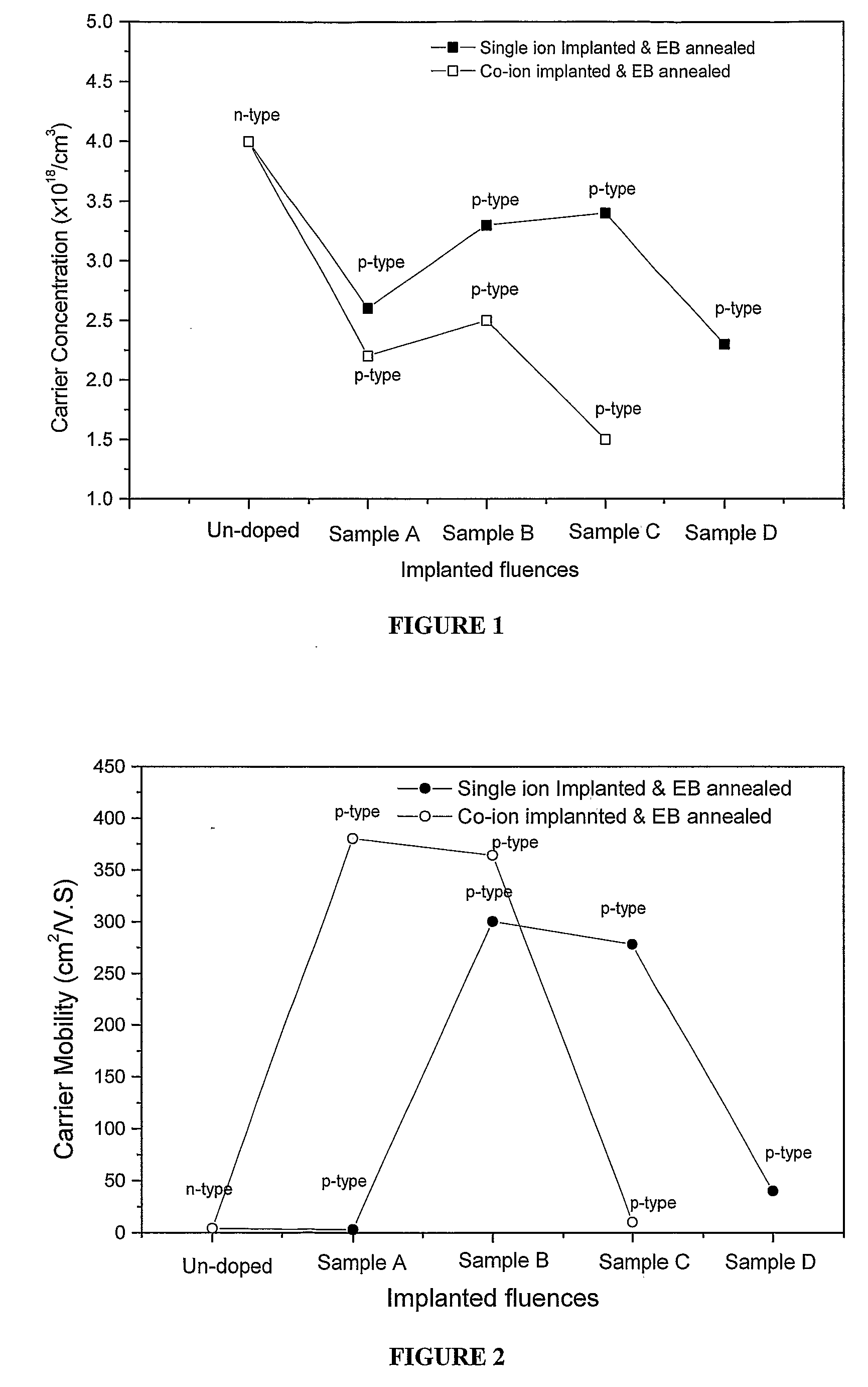
[0139]We took a 1×1 cm Si(100) substrate, mechanically cleaned it by spraying pressured air on to the surface and deposited a n-type ZnO thin film of around 300 nm. The targets were loaded into a high vacuum implantation chamber. 23 keV nitrogen ions (the acceptor) were implanted in an area of around 1 cm2 with various fluences starting from 1×10¹⁵ ions / cm2 to 5×10¹⁶ ions / cm2. The implantation depth was around 80 nm. The sample coded A corresponds to an implantation fluence of 1×10¹⁵ ions / cm2, which equates to around 0.2 atomic percent of N. The sample coded B corresponds to 2×10¹⁵ ions / cm2, which equates to around 0.4 atomic percent of N. The sample C corresponds to 2.5×10¹⁶ ions / cm2, which equates to around 5 atomic percent of N. The sample D corresponds to 5×10¹⁶ ions / cm2, which equates to around 10 atomic percent of N. After the implantation, the targets were annealed with a raster scanned electron beam at 800° C. for 15 minutes ...

example 2

ZnO film on SiO2 Substrate

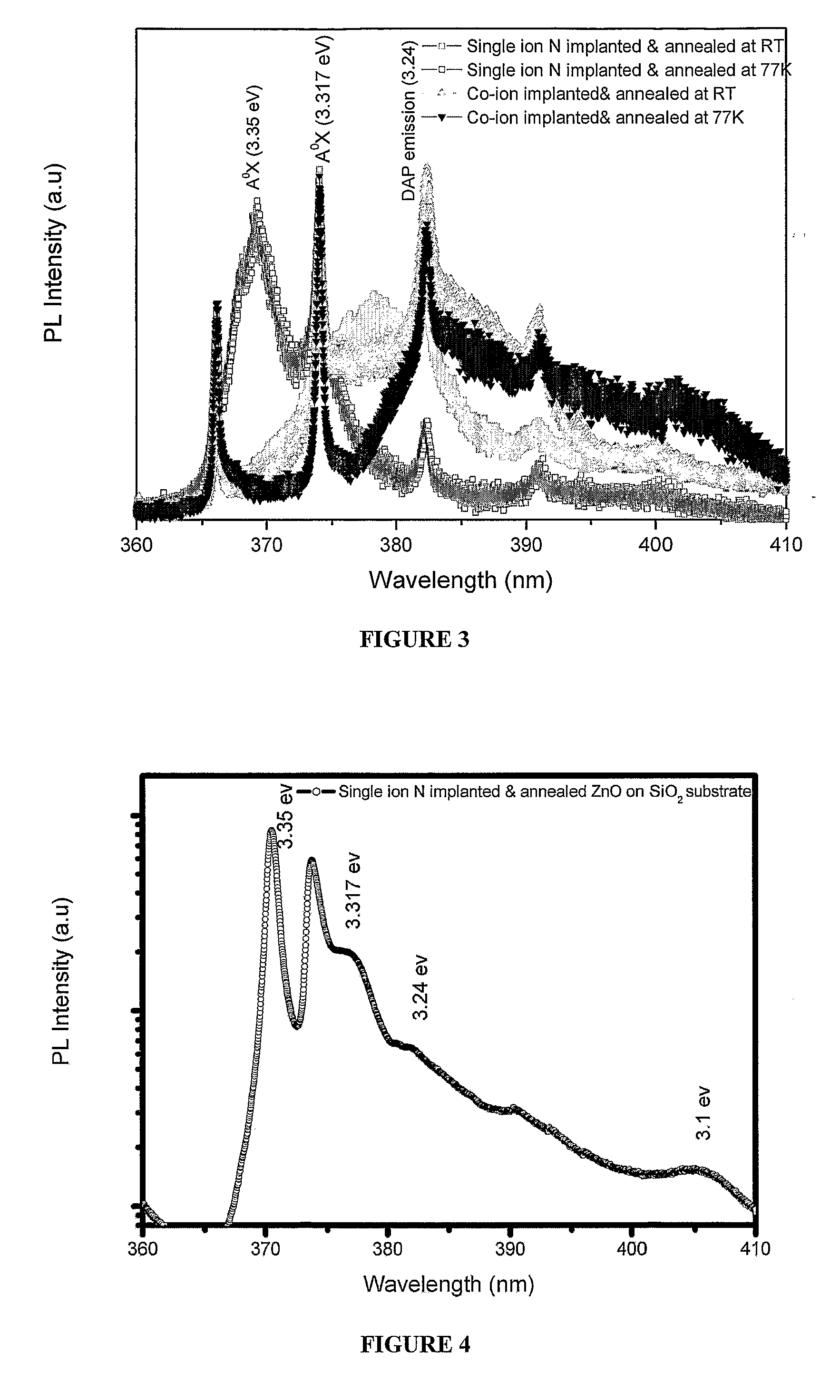
[0151]We took a 1×1 cm 500 nm thick silicon dioxide (SiO2, 100) on Si substrate, mechanically cleaned it by spraying pressured air on to the surface and deposited a n-type ZnO thin film of around 300 nm. The targets were loaded into a high vacuum implantation chamber. 23 keV nitrogen ions (the acceptor) were implanted in an area of around 1 cm2 with various fluences starting from 1×10¹⁵ ions / cm2 to 5×10¹⁶ ions / cm2. The implantation depth was around 80 nm. After the implantation, the targets were annealed with a raster scanned electron beam at 800° C. for 15 minutes with a temperature gradient of 5° C. / s.

[0152]The electrical properties of ZnO films deposited on SiO2, after implanting of the acceptor ion (nitrogen) and annealing, showed p-type carrier concentration values of 2×10¹⁷ to 4.0×1018 cm−3, hole mobilities of 1-100 cm2·Vs−1 and resistivities of 0.1-10 ohm·cm.

Photoluminescence (PL) Spectra

[0153]The optical properties of the ZnO films deposited on SiO2...

example 3

Bulk ZnO

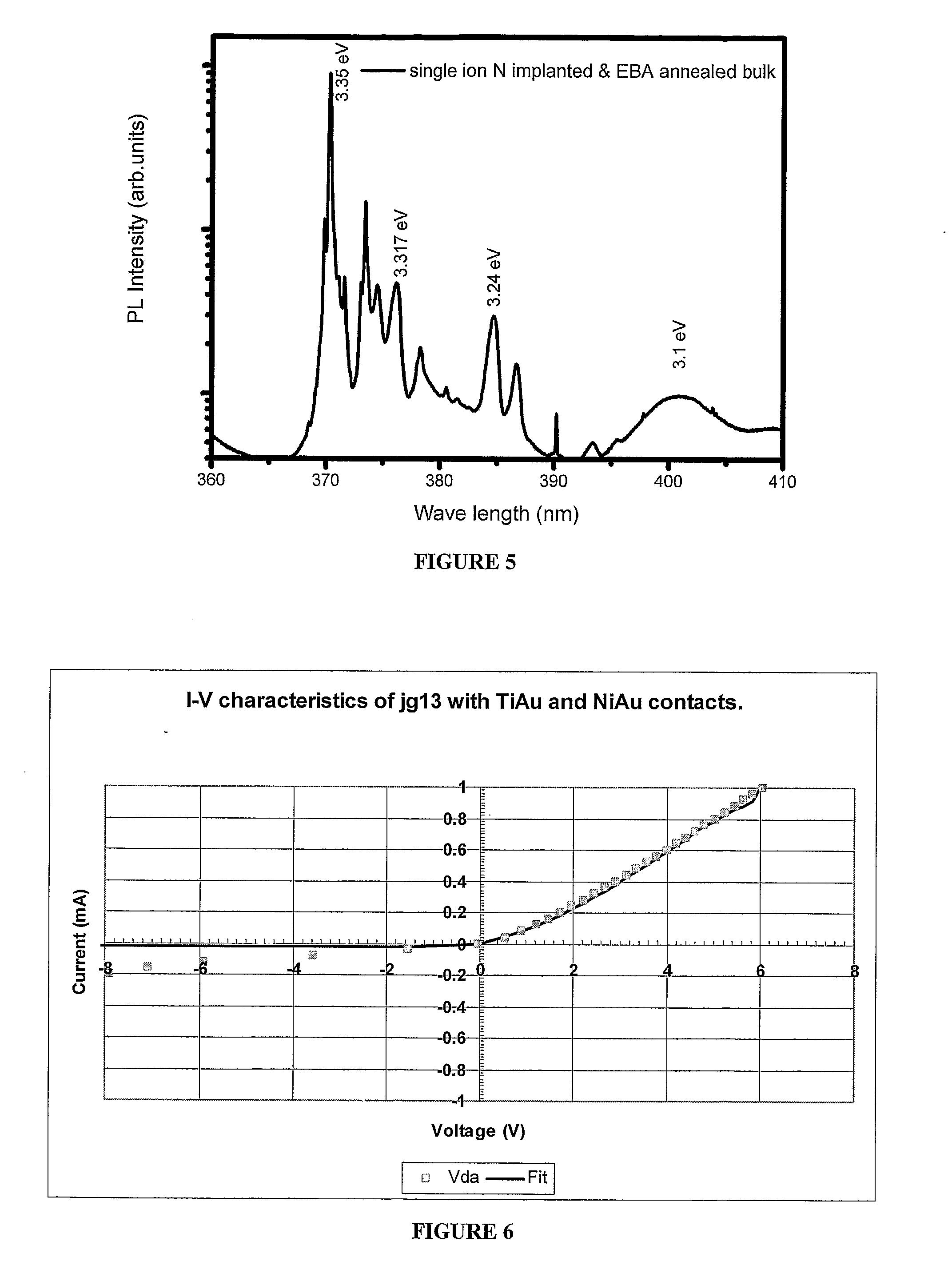
[0154]We took a 1×1 cm bulk n-type ZnO single crystal obtained from a commercial supplier. The targets were loaded into a high vacuum implantation chamber. 23 keV nitrogen ions (the acceptor) were implanted in an area of around 1 cm2 with various fluences starting from 1×10¹⁵ ions / cm2 to 5×10¹⁶ ions / cm2. The implantation depth was around 80 nm. After the implantation, the targets were annealed with the raster scanned electron beam at 800° C. for 15 minutes with a temperature gradient of 5° C. / s.

[0155]The electrical properties of the ZnO single crystal, after implantation of the acceptor ion (nitrogen) and annealing, showed p-type carrier concentration values of 1×10¹³ to 1.0×1018 cm−3, hole mobilities of 1-300 cm2·Vs−1 and resistivities of 0.01-100 ohm·cm. These properties are estimated from the properties determined for the ZnO thin films. Those persons skilled in the art will appreciate that some of the techniques used to characterise the thin films are not suitable for ch...


PUM


Abstract

A method for preparing p-type zinc oxide (ZnO) is described. The p-type ZnO is prepared by implanting low energy acceptor ions into an n-type ZnO substrate and annealing. In an alternative embodiment, the n-type ZnO substrate is pre-doped by implanting low energy donor ions. The p-type ZnO may have application in various optoelectronic devices, and a p-n junction formed from the p-type ZnO prepared as described above and a bulk n-type ZnO substrate is also described.

Description

TECHNICAL FIELD[0001]The present invention relates to zinc oxide semiconductor materials. More particularly, but not exclusively, it relates to the preparation of p-type zinc oxide.BACKGROUND ART[0002]Development of p-type conductivity zinc oxide (ZnO) materials has been identified as an emerging research and development initiative for next generation short-wavelength optoelectronic devices. When compared with materials that have been the subject of most research, such as gallium nitride (GaN), p-type ZnO has very promising electrical and optical properties that could prove superior in the development of optoelectronic devices.[0003]The main advantages of ZnO as a light emitter are its large exciton binding energy (60 meV), which provides optically efficient excitonic behaviour, and its wide band-gap. Both of these advantages are extremely valuable in optoelectronic applications. ZnO layers show n-type conductivity. However, the key challenges in developing ZnO technology for optoel...

Claims


Application Information

Patent Timeline
Patent Type & Authority Applications(United States)
IPC IPC(8): H01L21/425H01L33/00
CPCC01G9/02H01L33/0087H01L21/425
Inventor KENNEDY, JOHN VEDAMUTHUMARKWITZ, ANDREAS
Owner INST OF GEOLOGICAL & NUCLEAR SCI
Why Eureka
Try Eureka