Method and crucible for direct solidification of semiconductor grade multi-crystalline silicon ingots

a technology of multi-crystalline silicon and crucible, which is applied in the direction of crystallization separation, inorganic chemistry, crystal growth process, etc., can solve the problems of low possibility of controlling heat flux, limited heat removal rate, and hampered lateral direction, so as to increase the crystallization rate and stress in the crystalline silicon. , the effect of increasing the thermal gradien

Inactive Publication Date: 2009-08-20
REC SCANWAFER
View PDF5 Cites 8 Cited by
  • Summary
  • Abstract
  • Description
  • Claims
  • Application Information

AI Technical Summary

Benefits of technology

[0022]the wall thickness of the bottom of the crucible is dimensioned such that the thermal resistance across the bottom is reduced to a level of at least the same order as thermal resistance across the support below carrying the crucible or lower.
[0023]An increased rate of crystallization implies a larger thermal gradient across the crystallized silicon. This may cause increased stress in the crystalline silicon. However, thermal stress in the crystalline silicon may be minimised or even eliminated by ensuring that the heat flux is vertically oriented and linear. The situation where heat is extracted in such a way that the temperature gradients are linear within one material layer with respect to vertical position can be...

Problems solved by technology

The attainable rate of heat removal is limited by the great thermal resistance of the silica crucible.
Also, any attempt to vary the heat flux locally, e.g. in the lateral direction will be hampered by the very low possibility to control the heat flux.
This gives rise to thermal stresses and genera...

Method used


Image

  • Method and crucible for direct solidification of semiconductor grade multi-crystalline silicon ingots
  • Method and crucible for direct solidification of semiconductor grade multi-crystalline silicon ingots
  • Method and crucible for direct solidification of semiconductor grade multi-crystalline silicon ingots

Examples


example 1

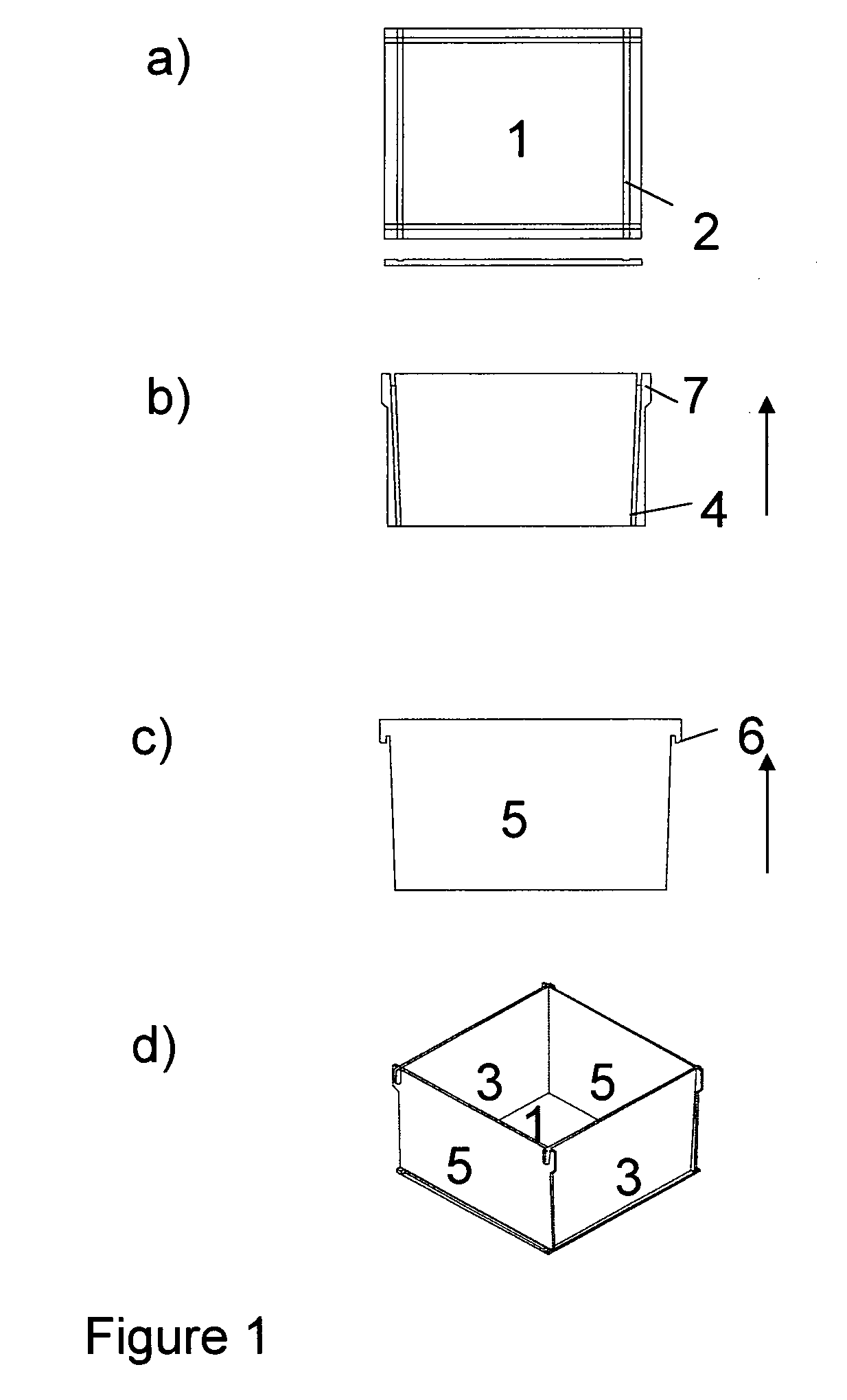
[0047]The crucible according to example 1 is schematically illustrated in FIG. 1a to 1d.

[0048]FIG. 1a illustrates the bottom plate 1, which is a quadratic plate with a groove 2 on the upward facing surface along each of its sides. The grove is fitted to the thickness of the side elements forming the walls of the crucible such that the lower edge of the side walls enters into the groove and forms a tight fitting. Alternatively, the side elements and the bottom groove may be given a complementary shape such as e.g. a plough and tongue.

[0049]FIG. 1b shows one rectangular wall element 3. There will be used two of these at opposing sides, see FIG. 1d. The side element 3 is equipped with a groove 4 along both edges on the surface facing inwards into the crucible. The grooves 4 are dimensioned to give a tight fitting with the side edges of the wall elements 5 placed perpendicularly on the wall elements 3. The grooves 4 and side edges of the wall elements 3 may be given an congruent angled...

example 2

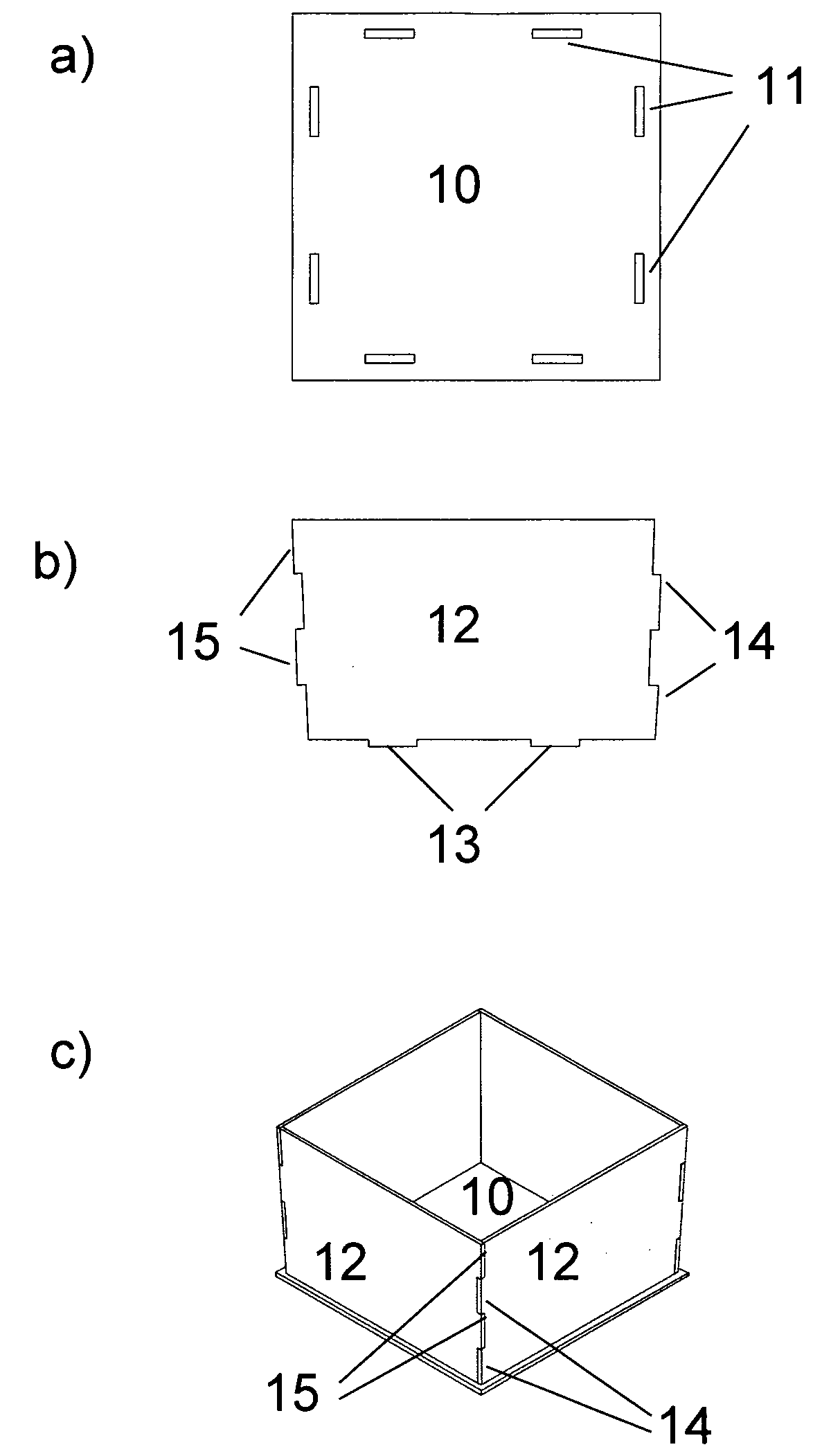
[0052]The crucible according to example 2 is schematically illustrated in FIG. 2a to 2c.

[0053]FIG. 2a illustrates the bottom plate 10, which is a quadratic plate with two elongated apertures 11 along each of its sides. The dimensions of the apertures are fitted such that they can receive a downward facing protrusion of the side walls and form a tight fitting. It is also envisioned to include grooves (not shown) running aligned with the centre axis of the apertures 11, similar to the grooves 2 of the bottom plate 1 of the first example.

[0054]FIG. 2b shows one wall element 12. There will be four of these elements, see FIG. 2c. The side element 12 is equipped with two protrusions 14, 15 on each side and two downward protrusions 13. The side protrusions are dimensioned such that the protrusion 14 enters the space between the protrusions 15 and forms a tight fitting when two wall elements 12 are assembled forming adjacent walls of the crucible. The downward facing protrusions 13 are dim...

example 3

Calculated Temperature Profile in a Furnace with Use of a Prior Art Silica Crucible

[0057]A calculation of a steady state one-dimensional temperature gradient at the start of crystallization with a standard furnace process is shown in FIG. 3. The temperature at the inside of the crucible bottom is 1415° C. The crucible bottom is 2 cm thick, and its thermal conductivity is 1.5 W / mK. The support plate is 60 mm thick, and its thermal conductivity is 80 W / mK. In order to remove 10 kW / m2, the temperature at the bottom of the support plate must be lowered to 1398° C. This rate of heat transfer can give crystallization rates up to 0.9 cm / h, depending on the amount of heat transported from the top chamber.


PUM

PropertyMeasurementUnit
Thicknessaaaaaaaaaa
Thermal resistanceaaaaaaaaaa
Heataaaaaaaaaa

Abstract

This invention relates to a method for direct solidification of semiconductor grade multi-crystalline silicon ingots allowing improved control with the solidification process and reduced levels of oxygen and carbon impurities in the ingot, by crystallizing the semiconductor grade silicon ingot, optionally also including the melting of the feed silicon material, in a crucible made of silicon nitride, or in a crucible made of a composite of silicon carbide and silicon nitride, and where the wall thickness of the bottom of the crucible is dimensioned such that the thermal resistance across the bottom is reduced to a level of at least the same order as thermal resistance across the support below carrying the crucible or lower. The invention also relates to crucibles which are made of silicon nitride, or of a composite of silicon carbide and silicon nitride, and where the wall thickness of the bottom of the crucible is dimensioned such that the thermal resistance across the bottom is reduced to a level of at least the same order as thermal resistance across the support below carrying the crucible or lower.

Description

[0001]This invention relates to a method for direct solidification of semiconductor grade multi-crystalline silicon ingots allowing improved control with the solidification process and reduced levels of oxygen and carbon impurities in the ingot. The invention also relates to crucibles enabling the method.BACKGROUND[0002]The world supplies of fossil oil are expected to be gradually exhausted in the following decades. This means that our main energy source for the last century will have to be replaced within a few decades, both to cover the present energy consumption and the coming increase in the global energy demand.[0003]In addition, many concerns are raised that the use of fossil energy increases the earth greenhouse effect to an extent that may turn dangerous. Thus the present consumption of fossil fuels should preferably be replaced by energy sources / carriers that are renewable and sustainable for our climate and environment.[0004]One such energy source is solar light, which irr...

Claims


Application Information

Patent Timeline
IPC IPC(8): C01B33/02B01D9/00B28B1/14
CPCC30B29/06C30B11/002C30B11/00F27B14/10
Inventor JULSRUD, STEINNAAS, TYKE LAURENCE
Owner REC SCANWAFER
Why Eureka
Try Eureka