Infinitely Stackable Interconnect Device and Method

a technology of interconnect devices and dice, which is applied in the direction of semiconductor devices, semiconductor/solid-state device details, electrical devices, etc., can solve the problems of difficulty and time-consuming steps, the difficulty of completing individual devices in chip form, and the inability to generalize the method allowing for unlimited number of dice to be stacked to form a complete system

Active Publication Date: 2009-08-27
THE BOARD OF TRUSTEES OF THE UNIV OF ARKANSAS
View PDF24 Cites 120 Cited by
  • Summary
  • Abstract
  • Description
  • Claims
  • Application Information

AI Technical Summary

Benefits of technology

[0050]A multi-functional capping chip accomplishes a generalized wafer-level and chip-scale packaging approach providing optical, electrical, fluidic and thermal through-substrate vias (TSV). The invention accommodates wafer-level packaging of a variety of devices including normal integrated circuit devices, but also devices including but not limited to biological or chemical sensors, optically active components, and Micro-Electro-Mechanical Systems. In this approach, a device wafer is fabricated in the normal manner. Since a device wafer normally includes top interconnect metallization, the inventive approach takes full advantage of such metallization for connection to a capping die. However, since it is important that such metallization be compatible with soldering, it may be required to modify the metallization materials on the device wafer. In addition, the design layout of the device wafer may be customized to the proposed process.

Problems solved by technology

It is commonly recognized that steps involving handling of individual devices in chip form are much more expensive than steps that are completed in wafer form.
This is due to the relative difficulty and time consuming steps involved in separately handling singulated chips.
However, no generalized method allowing for unlimited number of dice to be stacked to form a complete system has been proposed.
However, new challenges arise with 3D chip stacking, including requirements for chip-to-chip interconnect.
A particular problem that must be addressed with vertically stacked semiconductor dice is that of heat dissipation.
In fact, normal conductive or air convection methods of heat dissipation may be limiting.
As semiconductor dice clock speeds are steadily increased, limitations on signal propagation are being approached.
Electrical signal propagation is limited by parasitic resistances and capacitances, with associated “RC delay times”.
No good solution to these problems has been developed to date.
In addition, the need for good thermal management may lead to a requirement for high thermal conductivity materials; or high frequency devices may require ultra-low loss dielectrics.
One of the challenges that MEMS packaging faces is that the environments in which MEMS devices operate can vary dramatically with each application.
However, current implementations of MEMS and MOEMS devices, such as RF MEMS switches, or SOAC approaches are limited by lack of cost-effective and reliable packaging methods to accommodate the enclosed devices and to merge with current world-wide fabrication capabilities.
In recent years, costs of packaging and testing have dramatically increased from the norm of perhaps 10-20 percent of total cost, to 60-70 percent of total cost.
Responses to this steady shift in costs from integrated circuit to packaging and testing have been slow to arrive.
This method fails to meet the broad-based challenges inherent in device-level packaging in several respects.
Such approach is undesirable since the expense of forming through-substrate vias is roughly proportional to the depth of the via, but also because the lateral area consumed by such via increases in direct proportion to the thickness of the via.
While this problem could in principle be solved by simply increasing the 85 degree angle to 90 degrees, such slope is extremely difficult to metallize uniformly, leading to difficulties in filling the vias with conductive metal.
Third, the defined approach does not anticipate optical, fluidic or thermal vias.
Fourth, the approach does not define the capability to continue 3D stacking of die.
From these various problems, it is apparent that the method disclosed by Nagarajan et al is very limited in scope and that there is a need for a more universal solution accommodating a range of materials and functional domains.
Testing may occur before the device has been packaged; but since the package almost always affects performance, it is necessary to perform tests after encapsulation to verify that the original specifications and requirements have not been compromised beyond acceptable levels.
Choosing materials that are readily available and easily processed makes the task of high volume production easier, but these materials may not provide the performance needed for the device.
Conversely, exotic or rarely used materials that provide excellent performance may prove problematic in bringing the device to market due to high cost of manufacturing, difficulties in processing, or poor throughput or yield.
Whereas wirebonding interconnection has most frequently been the interconnect technology of choice, this technology is not extensible to 3D interconnections.
Both temperature, compression and ultrasonic energy may be incompatible with the enclosed devices.
In many devices that operate at high frequencies, such as greater than 1 gigahertz, parasitic capacitance and inductance limit performance, while dielectric losses lead to reduction of transmitted signals.
Devices which are interconnected primarily by wire bonds suffer from parasitics associated with the wire itself.
However, thermal dissipation paths are constrained to be along solder bumps that are designed to provide optimum electrical and mechanical connections, with little consideration for thermal dissipation.
In addition, maintaining a hermetic environment over a long period of time requires that all materials have very low outgassing rates, and may require the inclusion of active getters.
It is common to be concerned about the yield of devices, since cost is directly impacted by yield.
It is well known that by coupling a number of devices of unknown “goodness” into a system, the expectation is that the combined yield will suffer and costs will escalate.
For example, high frequency devices cannot be fully tested while in wafer form since the interconnections themselves become part of the circuitry.
Discrete devices may share a common substrate and cannot be accurately tested in wafer form since they are electrically connected.
Semiconductor dice fabrication is complex and expensive.

Method used


Image

  • Infinitely Stackable Interconnect Device and Method
  • Infinitely Stackable Interconnect Device and Method
  • Infinitely Stackable Interconnect Device and Method

Examples


first embodiment

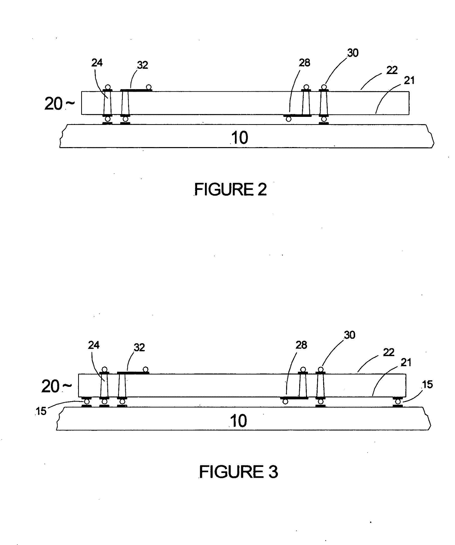
[0073]In the present invention, a multi-functional capping chip 20 is bonded to a device wafer 10 as shown in FIG. 2. A typical integrated circuit device wafer 10 may be connected by a multi-functional capping chip 20 to achieve redistribution of interconnection. This embodiment is advantageously employed when it is necessary to connect between two integrated circuit devices which do not have the same locations of bonding pads. Interconnection runners 28 on a first surface 21 of capping wafer 20 and interconnection runners 32 on a second surface 22 of multi-functional capping chip 20 are included to enable offsetting of bumps on first surface 21 from those on second surface 22.

[0074]In a second embodiment of the invention, a multi-functional capping chip 20 is bonded to a device wafer 10 as shown in FIG. 3. A sealing ring 15 may be included in order to hermetically or non-hermetically seal the integrated circuit portion from the environment. As in the first embodiment, this embodime...

sixth embodiment

[0078]In the invention, a multi-functional capping chip 20 is bonded to a device wafer 10 as shown in FIG. 7. As in the previous embodiments, a cavity 35 is included in order to provide appropriate relief for a moveable device, or to enclose biological, chemical or other materials; a sealing ring 15 may be included in order to hermetically seal the integrated circuit portion from the environment; an optical or fluidic via 40 is included; and active gettering materials 80 are also enclosed within cavity 35. In addition, optical element 45 is included in order to both control the direction and behavior of light rays passing through the multi-functional capping chip 20 and to hermetically seal optical and fluidic via 40. Optical element 45 may optionally be attached by adhesive layer 46.

seventh embodiment

[0079]In the invention, a multi-functional capping chip 20 is bonded to a device wafer 10 as shown in FIG. 8. As in the previous embodiments, a cavity 35 is included in order to provide appropriate relief for a moveable device, or to enclose biological, chemical or other materials; a sealing ring 15 may optionally be included in order to hermetically seal integrated circuit portion from the environment; an optical or fluidic via 40 is included; and active gettering materials 80 may optionally be enclosed within cavity 35. In addition, optical element 45 may be included in order to both control the direction and behavior of light rays passing through the multi-functional capping chip and to hermetically seal optical and fluidic via 40. In this embodiment, device wafer 10 is further prepared to have through substrate vias. Through substrate vias 60 are prepared, along with backside interconnection runners 72 and solder bumps 70. This embodiment is advantageously employed when it is ne...


PUM


Abstract

An infinitely stackable interconnect device and method having the capability for electrical, thermal, optical, and fluidic interconnections to various layers. Through-substrate vias in the interconnect device are filled to enable electrical and thermal connection or optionally hermetically sealed relative to other surfaces to enable fluidic or optical connection. Optionally, optical components may be placed within the via region in order to manipulate optical signals. Redistribution of electrical interconnection is accomplished on both top and bottom surfaces of the substrate of the interconnect chip. The method for fabricating the interconnect device includes the steps of: forming, insulating, and at least partially filling vias with conductive material; connecting vias to conductive traces on a top surface of the interconnect chip; connecting vias to conductive traces on a bottom surface of the interconnect chip; providing bump regions for electrical and mechanical interconnection to a subsequent interconnect device; and forming recessed regions to accommodate a subsequent die in a stack. The method simultaneously accomplishes interconnection and packaging of multiple semiconductor die to form a stack.

Description

TECHNICAL FIELD[0001]This invention relates generally to interconnection and packaging of semiconductor dice and specifically to a capping chip which may be placed on a previously fabricated device wafer, such as an integrated circuit or Micro-Electro-Mechanical Systems (MEMS) wafer. In a preferred embodiment the capping chip may be placed on a fully fabricated device wafer prior to dicing of said wafer, and may be heated appropriately to form a multiplicity of permanent electrical and mechanical connections. Electrical, optical, fluidic and thermal through-connections may be prepared on the multi-functional capping chip to enable interconnection between an underlying device chip and a second device chip, circuit chip or circuit board. The capping chip is flexible to accommodate either land grid array or ball grid array interconnections between a previously fabricated chip and a second previously fabricated chip or circuit board. The capping chip may incorporate recesses which can f...

Claims


Application Information

Patent Timeline
Patent Type & Authority Applications(United States)
IPC IPC(8): H01L23/538H01L21/50H01L23/522
CPCB81B7/0006B81B7/007H01L2924/12032H01L2924/1461H01L2924/15159H01L23/13H01L25/105H01L2924/01079H01L2924/09701H01L2224/16225H01L2924/15311H01L2924/15331H01L2924/12041H01L2225/1088H01L2225/1023H01L2225/1058H01L2924/00H01L2924/1627H01L2224/05009H01L2224/05548H01L2224/0557H01L2224/05573H01L2224/05568H01L2224/05001H01L2924/00014H01L2224/0554H01L2224/02377H01L2224/02379H01L24/05H01L2224/05599H01L2224/05099H01L2224/0555H01L2224/0556
Inventor FOSTER, RON B.MALSHE, AJAY P.KELLEY, MATTHEW W.
Owner THE BOARD OF TRUSTEES OF THE UNIV OF ARKANSAS
Why Eureka
Try Eureka