Semiconductor device and manufacturing method of the same

a technology of semiconductors and manufacturing methods, applied in the direction of transistors, basic electric elements, electric devices, etc., can solve the problems of gate electrodes obtained, production process also becomes difficult inevitably, and the control range of the threshold voltage is widened, so as to prevent the deterioration of the insulating layer during the formation of the second cap layer, the effect of preventing the reduction of the reliability of the insulating layer

Active Publication Date: 2009-09-03
RENESAS ELECTRONICS CORP
View PDF7 Cites 22 Cited by
  • Summary
  • Abstract
  • Description
  • Claims
  • Application Information

AI Technical Summary

Benefits of technology

[0032]The electrode conductive layer is thicker in the second conductivity type element region than in the first conductivity type element region so that diffusion of the second element into the electrode conductive layer and the insulating layer can be suppressed compared with the diffusion in the first conductivity type element region. For example, it is possible to diffuse the second element into the insulating layer in the second conductivity type element region but not to diffuse it into the insulating layer in the first conductivity type element region. By this, the insulating layer containing the first and second elements can be formed in the first conductivity type element region, while the insulating layer containing the first element can be formed in the second conductivity type element region. The threshold voltage of the first conductivity type semiconductor element and the threshold voltage of the second conductivity type semiconductor element can be controlled, respectively, whereby the control range of the threshold voltage can be widened.
[0033]The second cap layer is formed over the electrode conductive layer and the second cap layer and the insulating layer have therebetween the electrode conductive layer so that deterioration of the insulating layer during formation of the second cap layer can be prevented. This enables to prevent reduction in the reliability of the insulating layer due to deterioration thereof and thereby widen the control range of a threshold voltage while preventing reduction in the reliability of the insulating layer. For example, in the case of a MOS transistor in which a first conductivity type element and a second conductivity type element use an insulating layer as the gate insulating film thereof, reduction in the reliability of the gate insulating film can be prevented and at the same time, the control range of the threshold voltage can be widened. As a result, a highly reliable semiconductor device equipped with a first conductivity type semiconductor element and a second conductivity type semiconductor element having desired properties, respectively, can be manufactured easily.
[0034]According to the semiconductor device in one aspect of the invention, a first conductivity type semiconductor element contains first and second elements in a first element-added insulating layer thereof and contains the second element in an element-added conductive layer over the first element-added insulating layer. A second conductivity type semiconductor element contains the first element in a second element-added insulating layer thereof and is equipped with an electrode conductive layer over the second element-added insulating layer. Such a structure enables to realize the first conductivity type semiconductor element and the second conductivity type semiconductor element having threshold voltages suited therefor respectively. Since the first and second element-added insulating layers can be formed without etching on an insulating layer which is to be the first and second element-added insulating layers, deterioration in the manufacturing procedure can be prevented and reduction in reliability can therefore be prevented. As a result, a highly reliable semiconductor device equipped with a first conductivity type semiconductor element and a second conductivity type semiconductor element having desired properties, respectively, can be realized.
[0035]According to the semiconductor device in another aspect of the invention, a first conductivity type semiconductor element contains first and second elements in a first element-added insulating layer thereof and contains the second element in a first element-added conductive layer over the first element-added insulating layer. A second conductivity type semiconductor element contains the first element in a second element-added insulating layer thereof, is equipped with an electrode conductive layer over the second element-added insulating layer, and contains the second element in a second element-added conductive layer over the electrode conductive layer and another second element-added conductive layer. Such a structure enables to realize the first conductivity type semiconductor element and the second conductivity type semiconductor element having threshold voltages suited therefor respectively. Since the first and second element-added insulating layers can be formed without etching on an insulating layer which is to be the first and second element-added insulating layers, deterioration in the manufacturing procedure can be prevented and reduction in reliability can therefore be prevented. As a result, a highly reliable semiconductor device equipped with a first conductivity type semiconductor element and a second conductivity type semiconductor element having desired properties, respectively, can be realized.
[0036]According to the semiconductor device in a further aspect of the invention, a first conductivity type semiconductor element contains first and second elements in a first element-added insulating layer thereof and contains the second element in an element-added conductive layer over the first element-added insulating layer. A second conductivity type semiconductor element contains the first element in a second element-added insulating layer thereof, is equipped with an electrode conductive layer over the second element-added insulating layer, and contains the second element in a second element-added conductive layer over the electrode conductive layer and another second element-added conductive layer. Such a structure enables to realize the first conductivity type semiconductor element and the second conductivity type semiconductor element having threshold voltages suited therefor respectively. Since the first and second element-added insulating layers can be formed without etching on an insulating layer which is to be the first and second element-added insulating layers, deterioration in the manufacturing procedure can be prevented and reduction in reliability can therefore be prevented. As a result, a highly reliable semiconductor device equipped with a first conductivity type semiconductor element and a second conductivity type semiconductor element having desired properties, respectively, can be realized.
[0037]According to the semiconductor device in a still further aspect of the invention, a first conductivity type semiconductor element contains first and second elements in a first element-added insulating layer thereof and contains the second element in a first element-added conductive layer over the first element-added insulating layer. A second conductivity type semiconductor element contains the first element in a second element-added insulating layer thereof, is equipped with an electrode conductive layer over the second element-added insulating layer, and has an upper conductive layer containing a material different from that of the electrode conductive layer over the electrode conductive layer. Such a structure enables to realize the first conductivity type semiconductor element and the second conductivity type semiconductor element having threshold voltages suited therefor respectively. Since the first and second element-added insulating layers can be formed without etching on an insulating layer which is to be the first and second element-added insulating layers, deterioration in the manufacturing procedure can be prevented and reduction in reliability can therefore be prevented. As a result, a highly reliable semiconductor device equipped with a first conductivity type semiconductor element and a second conductivity type semiconductor element having desired properties, respectively, can be realized.

Problems solved by technology

Formation of pMOSFET and nMOSFET by using at least two materials utterly different from each other in physical properties, respectively, is however presumed to complicate the production flow.
Even if materials of the same kind are used as described in Japanese Patent Laid-Open Nos. 2007-242894, 2007-141889, 2005-294799, and 2007-142153, the production process also becomes difficult inevitably.
Moreover, when different metal materials are used for pMOSFET and nMOSFET, respectively, gate electrodes obtained by simultaneous etching or the like of different materials on one chip (wafer) cannot easily have a satisfactory gate shape.
There is therefore a danger of not obtaining desired device characteristics.
This may lead to failure in obtaining desired device characteristics and become a problem to be overcome.
The etching step of this metal layer is performed immediately above the gate insulating film so that it may damage the gate insulating film.
There is therefore a danger of reducing the reliability of the device.
224(2006), formation and removal steps of a capping layer are repeated on the gate insulating film so that there is a danger of deterioration in the gate insulating film and reduction in the reliability of the resulting device.

Method used


Image

  • Semiconductor device and manufacturing method of the same
  • Semiconductor device and manufacturing method of the same
  • Semiconductor device and manufacturing method of the same

Examples


first embodiment

[0102]Then, as in the first embodiment, a poly-Si layer is deposited to give a thickness within a range of from 30 to 120 nm and each gate electrode of the pFET and the nFET is processed by dry etching or the like. Also in this embodiment, use of the same main material for the gate electrodes of the nFET and the pFET facilitates processing of the gate electrodes. As a result, as illustrated in FIG. 12, a dual gate electrode structure, in which the gate electrode of the nFET has a stack structure of the gate-electrode metal film M and the poly-Si layer 10 and the gate electrode of the pFET has a stack structure of the p-side gate-electrode metal film MB and the poly-Si layer 10, is formed.

[0103]As in the first embodiment, ordinary process flows for CMOS formation are conducted successively to complete the CMOS.

[0104]Also this embodiment does not require formation of the poly-Si layer 10.

[0105]As described above, according to this embodiment, a CMOS permitting operation of the nFET an...

second embodiment

[0111]As in the first or second embodiment, ordinary process flows for CMOS formation are conducted successively to complete the CMOS.

[0112]As described above, according to this embodiment, a CMOS permitting the nFET and the pFET to operate at desired threshold voltages, respectively can be formed easily with accuracy by having a dual gate electrode structure in which the gate electrode GE of the nFET has the n-side gate-electrode metal film MA and the gate electrode GE of the pFET has the p-side gate-electrode metal film MC, thus having work functions different from each other. In particular, since main materials used for the gate electrodes are the same between the nFET and the pFET, the gate electrodes can be processed more easily by etching or the like. This enables improvement in the processing accuracy of a minute gate electrode. In addition, a step of removing the gate electrode from one channel region which is employed in the conventional hybrid metal gate electrode structur...

third embodiment

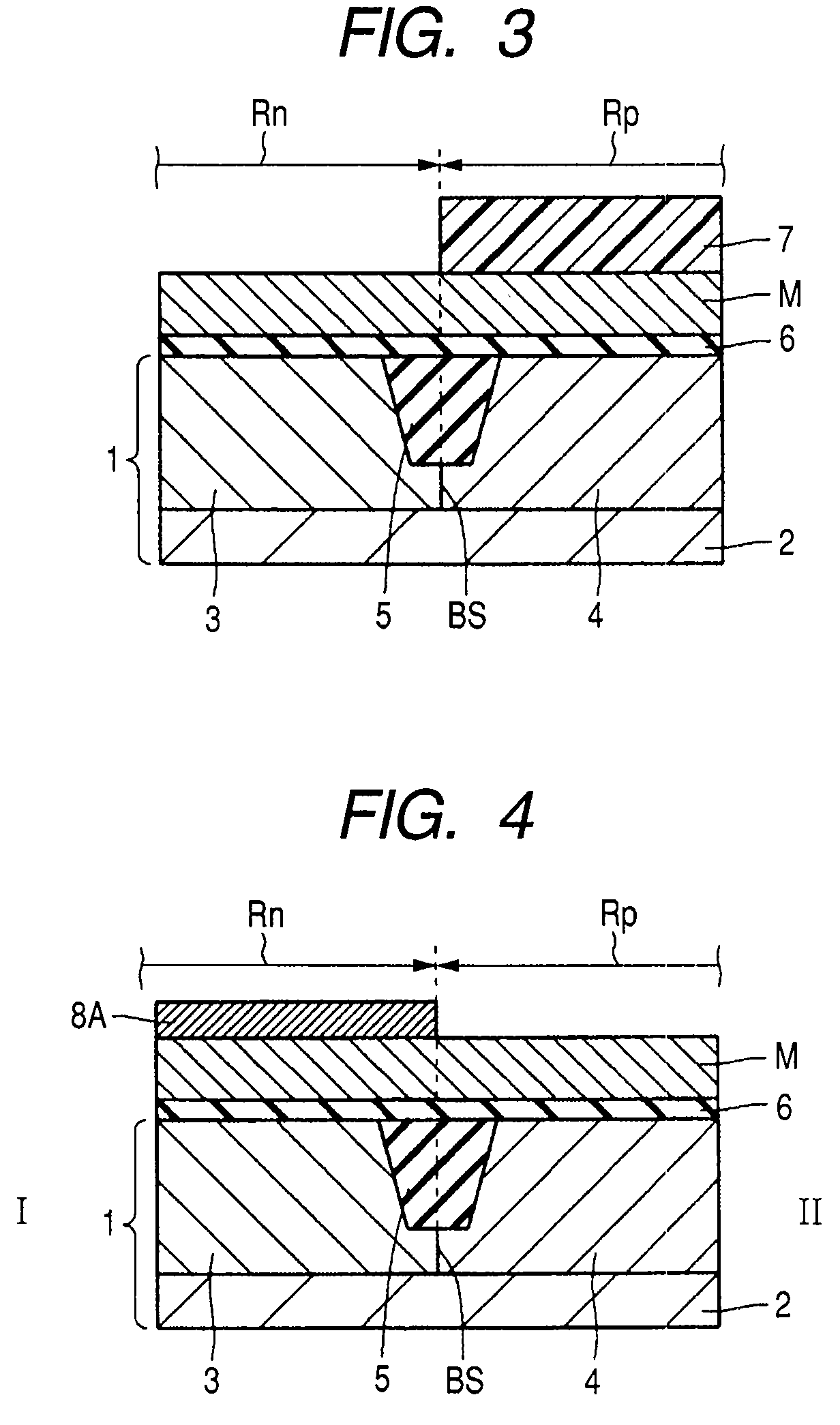
[0120]When the present embodiment is applied to the method of the third embodiment illustrated in FIGS. 13 and 14, an n-side gate-electrode metal film MA and a p-side gate-electrode metal film MC are formed as illustrated in FIG. 14, followed by the formation of a second gate-electrode metal film N over the entire upper surfaces of the n-side gate-electrode metal film MA and the p-side gate-electrode metal film MC as illustrated in FIG. 24.

[0121]When the present embodiment is applied to the method of the third embodiment illustrated in FIG. 15, after formation of the n-side cap layer 8A and the second p-side cap layer 8C as illustrated in FIG. 15 but prior to diffusion of the n-side cap layer 8A and the second p-side cap layer 8C, a second gate-electrode metal film N is formed over the entire upper surfaces of the n-side cap layer 8A and the second p-side cap layer 8C as illustrated in FIG. 25.

[0122]As described above, the present embodiment can provide the following advantages. Fir...


PUM

PropertyMeasurementUnit
thicknessaaaaaaaaaa
thicknessaaaaaaaaaa
thicknessaaaaaaaaaa

Abstract

Provided is a highly reliable semiconductor device equipped with a plurality of semiconductor elements having desired properties, respectively; and a manufacturing method facilitating the manufacture of the semiconductor device. The semiconductor device is manufactured by forming a gate-electrode metal film having a thickness of from 3 to 30 nm over the entire upper surface of a gate insulating film; forming an n-side cap layer having a thickness of 10 nm or less over the entire upper surface of a portion of the gate-electrode metal film belonging to an nFET region by using a material different from that of the gate-electrode metal film; and carrying out heat treatment over the n-side cap layer to diffuse the material of the n-side cap layer into the gate-electrode metal film immediately below the n-side cap layer and react them to form an n-side gate-electrode metal film in a nFET region. A poly-Si layer is then deposited, followed by gate electrode processing.

Description

CROSS-REFERENCE TO RELATED APPLICATIONS [0001]The disclosures of Japanese Patent Applications No. 2008-93306 filed on Mar. 31, 2008, No. 2008-47462 filed on Feb. 28, 2008, and No. 2008-273763 filed on Oct. 24, 2008 including the specification drawings and abstract are incorporated herein by reference in its entirety.BACKGROUND OF THE INVENTION[0002]The present invention relates to a semiconductor device and a manufacturing method thereof, more specifically, a semiconductor device having a plurality of gate electrode structures and a manufacturing method thereof.[0003]In CMOS devices after 45-nm node ones, replacement of a structure having poly-Si as a gate electrode and SiON as a gate insulating film with a gate stack structure having a high-dielectric-constant insulating film (which will hereinafter be called “high-k film”) as the gate insulating film has been started. This replacement occurs because compared with a SiO2 film or the like, a high-k film functions as a thin film duri...

Claims


Application Information

Patent Timeline
Patent Type & Authority Applications(United States)
IPC IPC(8): H01L27/092H01L21/3205
CPCH01L21/823842
Inventor SAKASHITA, SHINSUKEKAWAHARA, TAKAAKIYUGAMI, JIRO
Owner RENESAS ELECTRONICS CORP
Why Eureka
Try Eureka