Etch rate and critical dimension uniformity by selection of focus ring material

a focus ring and material technology, applied in the direction of basic electric elements, electrical equipment, electric discharge tubes, etc., can solve the problems of increasing the importance of residual non-uniformity and the difficulty of maintaining cd uniformity across the substrate during the etching process

Inactive Publication Date: 2009-09-03
APPLIED MATERIALS INC
View PDF12 Cites 17 Cited by
  • Summary
  • Abstract
  • Description
  • Claims
  • Application Information

AI Technical Summary

Problems solved by technology

As feature size shrinks, manufacturers are challenged to maintain control of device properties and performance.
As structures are formed closer to the edge, maintaining CD uniformity across the substrate during etching processes becomes more difficult.
Quartz, however, allows residual non-uniformity that becomes increasingly important as devices, and edge-exclusion, become smaller.

Method used


Image

  • Etch rate and critical dimension uniformity by selection of focus ring material
  • Etch rate and critical dimension uniformity by selection of focus ring material
  • Etch rate and critical dimension uniformity by selection of focus ring material

Examples


Embodiment Construction

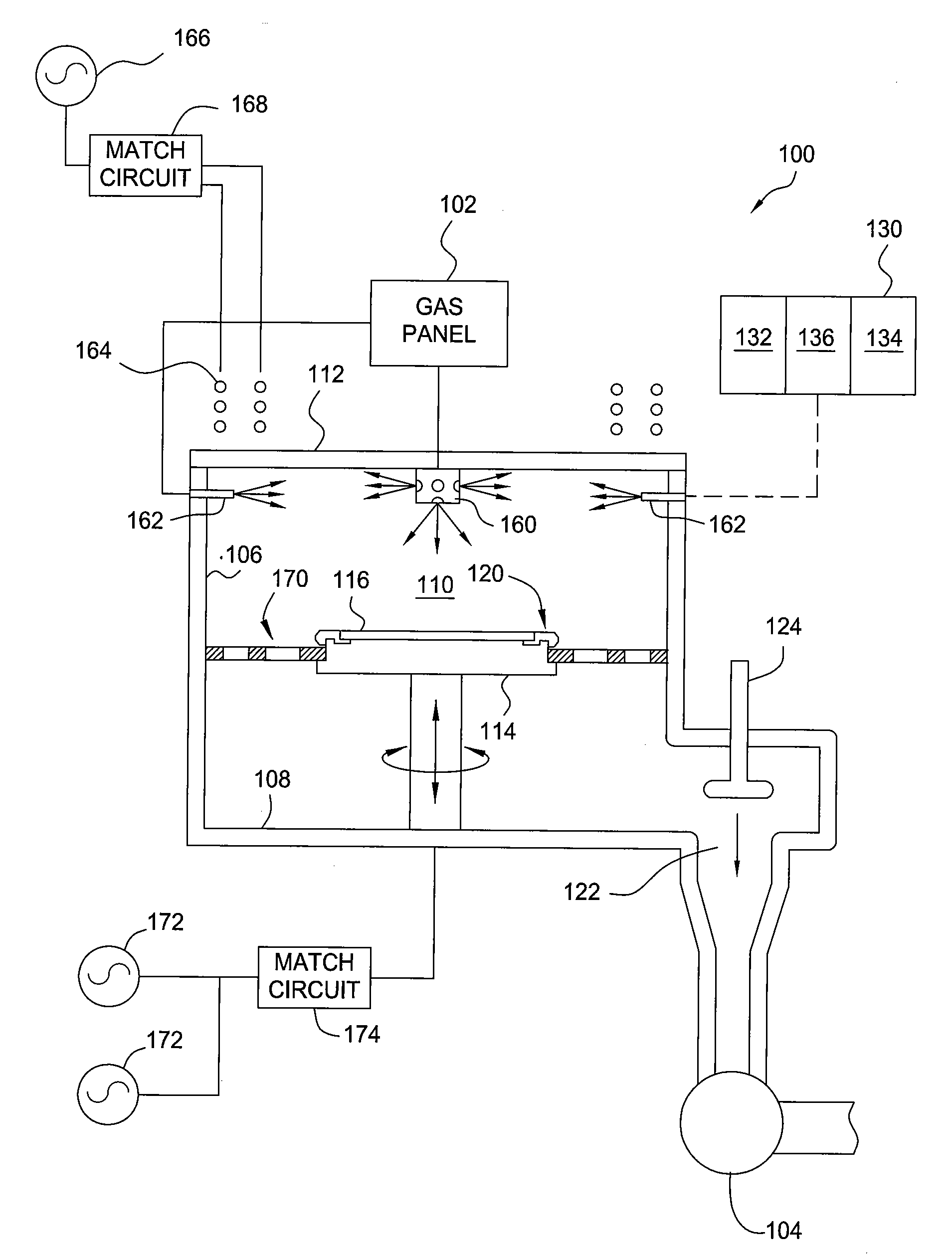
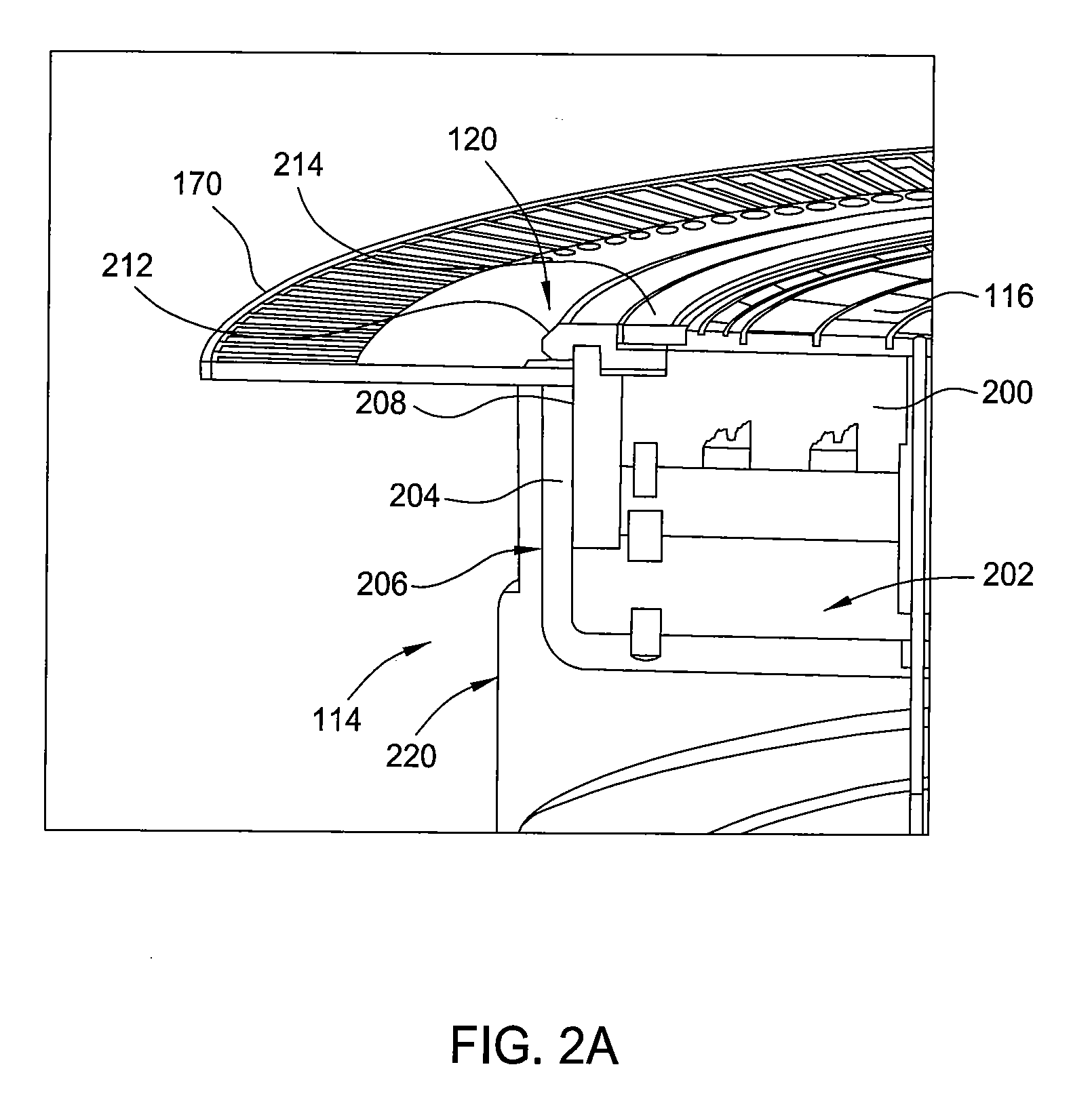
[0019]Embodiments of the invention generally provide a chamber for etching a substrate in a semiconductor manufacturing process. FIG. 1 is a schematic cross-sectional view of an exemplary process chamber 100 having a focus ring assembly 120 according to one embodiment of the invention. The process chamber 100 has a chamber body comprising sidewalls 106 and a bottom 108 that partially define a process volume 110 upwardly closed by a lid 112. The process chamber 100 is coupled to a gas panel 102, a vacuum pump 104, and a controller 130. A substrate support assembly 114 with a substrate support 116 is provided approximately at a central region of the process volume 110 to support a substrate (not shown) during processing. The focus ring assembly 120 is supported on the substrate support assembly 114 and circumscribes the substrate. One or more gas distributors are disposed in the chamber above the substrate support assembly 114 to provide process and other gases into the process volume...


PUM

PropertyMeasurementUnit
angleaaaaaaaaaa
angleaaaaaaaaaa
angleaaaaaaaaaa

Abstract

A method and apparatus are provided for plasma etching a substrate in a processing chamber. A focus ring assembly circumscribes a substrate support, providing uniform processing conditions near the edge of the substrate. The focus ring assembly comprises two rings, a first ring and a second ring, the first ring comprising quartz, and the second ring comprising monocrystalline silicon, silicon carbide, silicon nitride, silicon oxycarbide, silicon oxynitride, or combinations thereof. The second ring is disposed above the first ring near the edge of the substrate, and creates a uniform electric field and gas composition above the edge of the substrate that results in uniform etching across the substrate surface.

Description

CROSS-REFERENCE TO RELATED APPLICATIONS[0001]This application claims benefit of U.S. provisional patent application Ser. No. 61 / 032,920, filed Feb. 29, 2008, which is herein incorporated by reference.BACKGROUND OF THE INVENTION[0002]1. Field[0003]Embodiments of the present invention relate to the field of semiconductor substrate processing system. More specifically, the invention relates to a focus ring assembly suitable for use in a substrate process chamber.[0004]2. Description of the Related Art[0005]For more than half a century, the semiconductor industry has followed Moore's Law, which states that the density of transistors on an integrated circuit doubles about every two years. Continued evolution of the industry along this path will require smaller features patterned onto substrates. As feature size shrinks, manufacturers are challenged to maintain control of device properties and performance. Maintaining control of critical dimensions of features on a semiconductor substrate...

Claims


Application Information

Patent Timeline
Patent Type & Authority Applications(United States)
IPC IPC(8): H01L21/3065C23F1/08
CPCH01J37/3244H01J37/32623H01L21/68735H01L21/67069H01J37/32642H01J37/321H01J2237/334
Inventor HAMMOND, IV, EDWARD P.ZOU, JINGBELEN, RODOLFO P.SHEN, MEIHUAGANI, NICOLASNGUYEN, ANDREWPALAGASHVILI, DAVIDWILLWERTH, MICHAEL D.
Owner APPLIED MATERIALS INC
Why Eureka
Try Eureka