Solar cell and fabrication method using crystalline silicon based on lower grade feedstock materials

a technology of crystalline silicon and feedstock materials, applied in the field of photovoltaic devices, can solve the problems of high serial resistance and/or low shunt resistance, inability to achieve the desired results with a single process, and inability to meet the requirements of the application, etc., to achieve the effect of increasing the output of electricity, low resistance and increasing the efficiency of solar energy technologies

Inactive Publication Date: 2009-09-10
SILICOR MATERIALS INC
View PDF13 Cites 77 Cited by
  • Summary
  • Abstract
  • Description
  • Claims
  • Application Information

AI Technical Summary

Benefits of technology

[0056]The process and system features and functions described herein, therefore, form a low resistance solar cell metallization and metallization formation method. Stepping back a bit, photovoltaic or solar cells, formed consistent with the teachings of the present disclosure may be aligned as an array with various panels fitted along a mounting system. One of the main advantages is the ability of such an array includes the ability to combine various numbers of cells to provide a greater output of electricity. This makes solar electricity a viable option to power small homes and businesses.
[0057]With the cost advantages of using UMG silicon, as here described, the increasing efficiency of solar energy technologies, it is possible to purchase and install panel harnessing energy from the sun's rays. The costs involved with supplying electricity from a solar array using the teaching here disclosed may provide a substantial amount of electricity, reducing future electricity generation costs and consumer energy expenditures.

Problems solved by technology

In using UMG or silicon feedstock, with similar quality additional process constraints may arise.
Secondly, the process seeks to diffuse hydrogen from the ARC into the p-doped bulk silicon for defect passivation.
As such, it is generally not practical or optimal to achieve the desired results with a single process.
If the temperature process is not adjusted correctly, high serial resistance and / or low shunt resistance will result.
Reasons may include metal penetration into the bulk silicon, poor formation of Ag crystallites in the n-doped region and / or poor intergrowth of these Ag crystallites with the Ag fingers.
), the BSF quality generally decreases, principally due to inhomogeneity problems, and wafer bowing can become critical.
While there may be Al pastes that allow higher firing temperatures, even with these improvements, the duration at such temperature can only be in the range of several seconds.
At the same time, using two firing processes yet results in an ineffective solar cell.
Another limitation of known solar cell formation processes relates to the use of firing processes with solar cells using UMG silicon.
In order to use UMG silicon, however, novel defect engineering processes are required.
This is so, because doing so may reverse or adversely affect the defect engineering results.

Method used


Image

  • Solar cell and fabrication method using crystalline silicon based on lower grade feedstock materials
  • Solar cell and fabrication method using crystalline silicon based on lower grade feedstock materials
  • Solar cell and fabrication method using crystalline silicon based on lower grade feedstock materials

Examples


Embodiment Construction

[0030]In the present specification, an embodiment showing a singular component should not be considered limiting; rather, the invention is intended to encompass other embodiments including a plurality of the same component, and vice-versa, unless explicitly stated otherwise herein. Moreover, applicants do not intend for any term in the specification or claims to be ascribed an uncommon or special meaning unless explicitly set forth as such. Further, the present invention encompasses present and future known equivalents to the known components referred to herein by way of illustration.

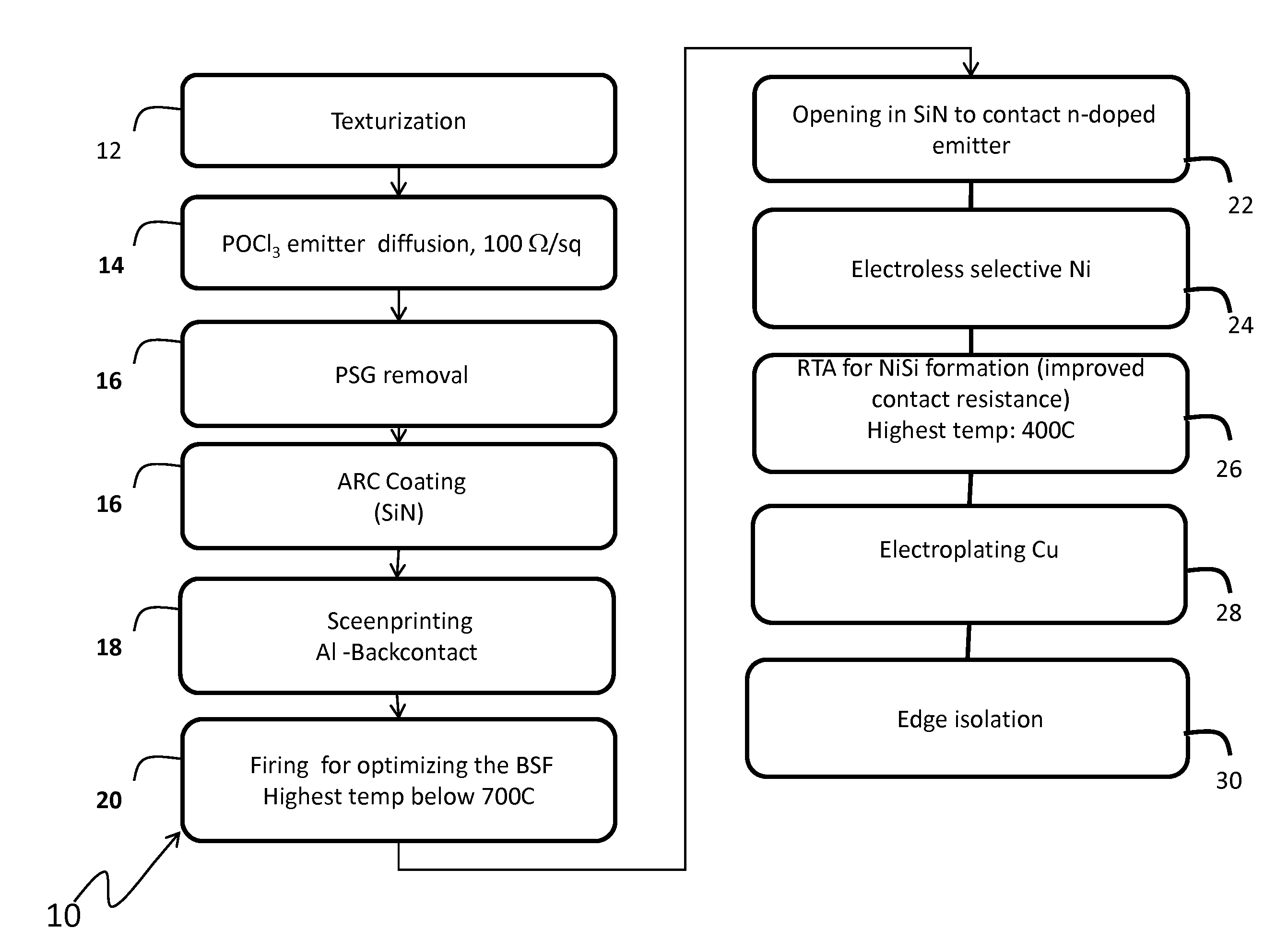
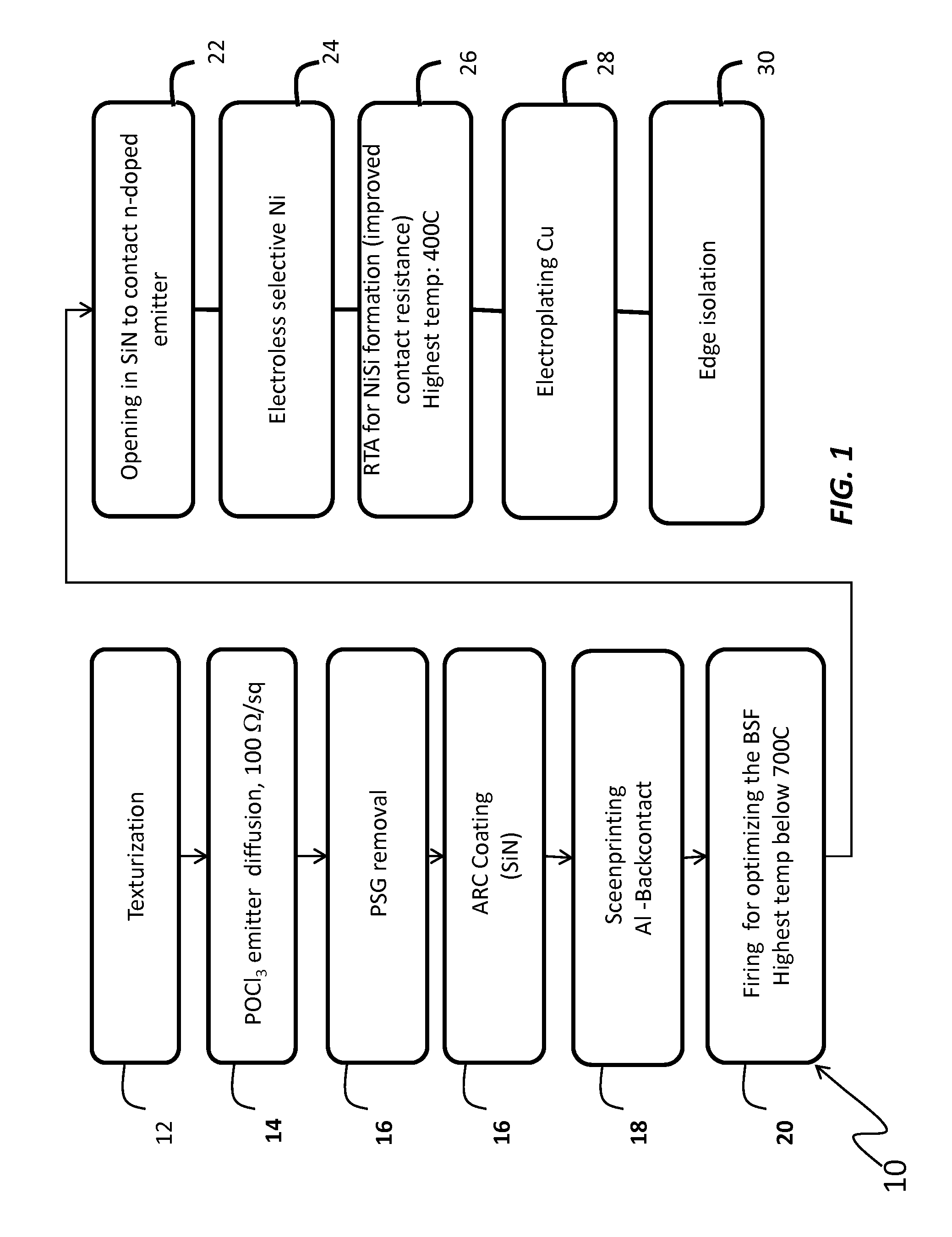
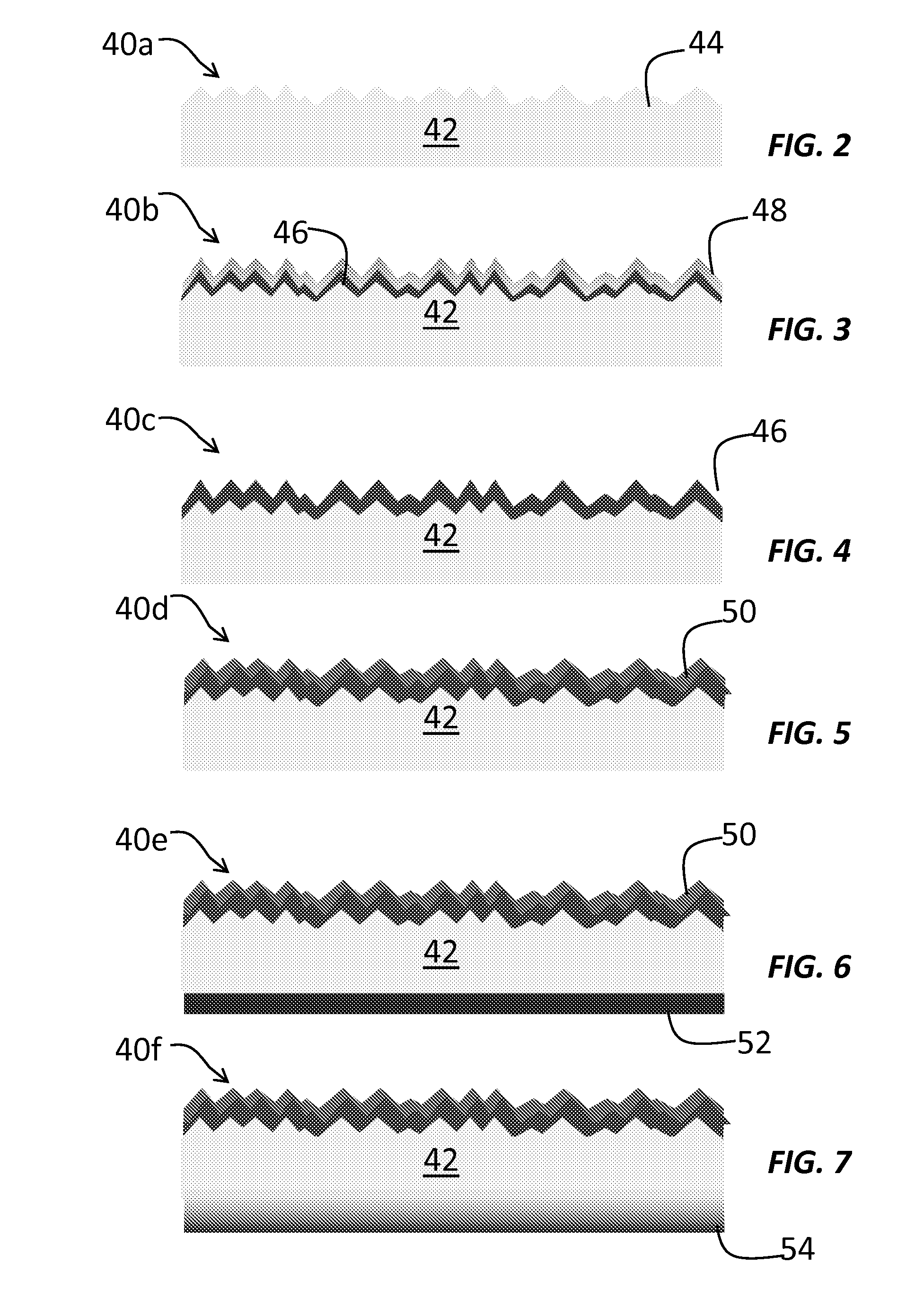
[0031]The method and system of the present disclosure provide a method for forming a low resistance metallization in the formation of a solar cell. Although the present disclosure has particular application in solar cells formed using UMG silicon, it should be understood that the present disclosure may further apply to any form of silicon, including float zone silicon, Czochralski silicon, magnetic Czoc...


PUM

PropertyMeasurementUnit
temperatureaaaaaaaaaa

Abstract

Formation of a solar cell device from upgraded metallurgical grade silicon which has received at least one defect engineering process and including a low contact resistance electrical path. An anti-reflective coating is formed on an emitter layer and back contacts are formed on a back surface of the bulk silicon substrate. This photovoltaic device may be fired to form a back surface field at a temperature sufficiently low to avoid reversal of previous defect engineering processes. The process further forms openings in the anti-reflective coating and a low contact resistance metal layer, such as nickel layer, over the openings in the anti-reflective coating. The process may anneal the low contact resistance metal layer to form n-doped portion and complete an electrically conduct path to the n-doped layer. This low temperature metallization (e.g., <700° C.) supports the use of UMG silicon for the solar device formation without the risk of reversing earlier defect engineering processes.

Description

FIELD[0001]The present invention relates generally to photovoltaic devices, and more particularly to a system and method for making an improved solar cell derived from crystalline silicon based on lower grade feedstock materials.DESCRIPTION OF THE RELATED ART[0002]Photovoltaic solar cells directly convert radiant energy from the sun into electrical energy. Photovoltaic cells can be aligned as an array that aligns various numbers of cells to provide a greater output of electricity. This makes solar electricity a viable option to power small homes and businesses.[0003]The manufacture of photovoltaic solar cells involves use of semiconductor substrates in the form of sheets or wafers having a shallow p-n junction adjacent one surface, commonly called the “front side.” The solar cell substrate may be of polycrystalline silicon having p-type conductivity and a p-n junction located about 0.3-0.5 microns from its front side, and having a silicon nitride coating approximately 80 nm (dependi...

Claims


Application Information

Patent Timeline
Patent Type & Authority Applications(United States)
IPC IPC(8): H01L31/042H01L31/00
CPCC23C18/1603C23C18/32C25D7/12H01L31/02168H01L31/022425Y02E10/547H01L31/068H01L31/1864C23C18/1605C23C18/1653C23C18/1692H01L31/0236H01L31/02245H01L31/1804H01L31/02363Y02P70/50C25D7/126
Inventor OUNADJELA, KAMELRAKOTONIAINA, JEAN PATRICEKAES, MARTINZICKERMANN, DIRKBLOSSE, ALAINZERGA, ABDELLATIFHEUER, MATTHIASKIRSCHT, FRITZ
Owner SILICOR MATERIALS INC
Why Eureka
Try Eureka