Electronic device, process for producing the same and electronic equipment making use thereof

a technology of electronic equipment and electrodes, applied in thermoelectric devices, instruments, material analysis, etc., can solve the problems of high driving voltage applied to device elements, difficult to obtain bulk properties, and difficult to obtain desired functions, so as to reduce the connection resistance between the electrode and the conductive organic molecule layer, the effect of reducing the variation of the connection resistan

Active Publication Date: 2009-09-10
PANASONIC CORP
View PDF7 Cites 5 Cited by
  • Summary
  • Abstract
  • Description
  • Claims
  • Application Information

AI Technical Summary

Benefits of technology

[0013]In the electronic device of the present invention, since the second organic molecules are disposed on the electrode surface in order to align the direction of the π conjugate planes formed by the conjugated π electrons, a stable charge transfer utilizing overlaps between the second organic molecule and the π conjugate planes of the adjacent first organic molecule is achieved. As a result, the connection resistance between the electrode and the conductive organic molecule layer, and its variations, can be reduced. In addition, since the second organic molecule is bonded chemically to the electrode, interfacial peeling and the like can be restricted. Thus, according to the present invention, an electronic device (an organic electronic device) having low connection resistance between an electrode and a conductive organic molecule layer and having the connection resistance with small variations can be obtained. In the case of the electronic device of the present invention being a TFT, a TFT having a low driving voltage can be obtained. Since the electronic device of the present invention does not require patterning the organic molecule layer formed on the electrode, it is manufactured easily. Since the electronic apparatus of the present invention uses the electronic device of the present invention (TFT), it has characteristics such as flexibility.

Problems solved by technology

When the scale of miniaturization reaches the utmost limit, it becomes impossible to obtain the bulk properties and difficult to obtain a desired function.
However, the organic semiconductors already been reported to have problems, such as having lower carrier mobility than those of inorganic semiconductors and causing high driving voltage when applied to device elements.
In most organic electronic devices that employ conductive organic molecules, sufficient device characteristics expected from the properties of conductive organic molecules can not be obtained.
In addition, conventional techniques did not achieve sufficient improvement in electric connectivity between an electrode and an organic molecule layer, and thus a wide range of variations was found in the obtained characteristics in some cases.

Method used


Image

  • Electronic device, process for producing the same and electronic equipment making use thereof
  • Electronic device, process for producing the same and electronic equipment making use thereof
  • Electronic device, process for producing the same and electronic equipment making use thereof

Examples


embodiment 1

[0091]In Embodiment 1, a case in which an oligothiophene derivative is employed as the first organic molecule composing the semiconductor layer of the TFT is described.

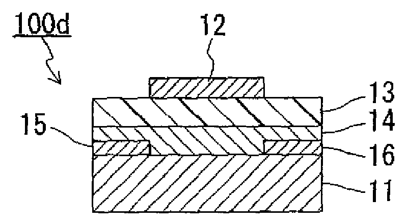
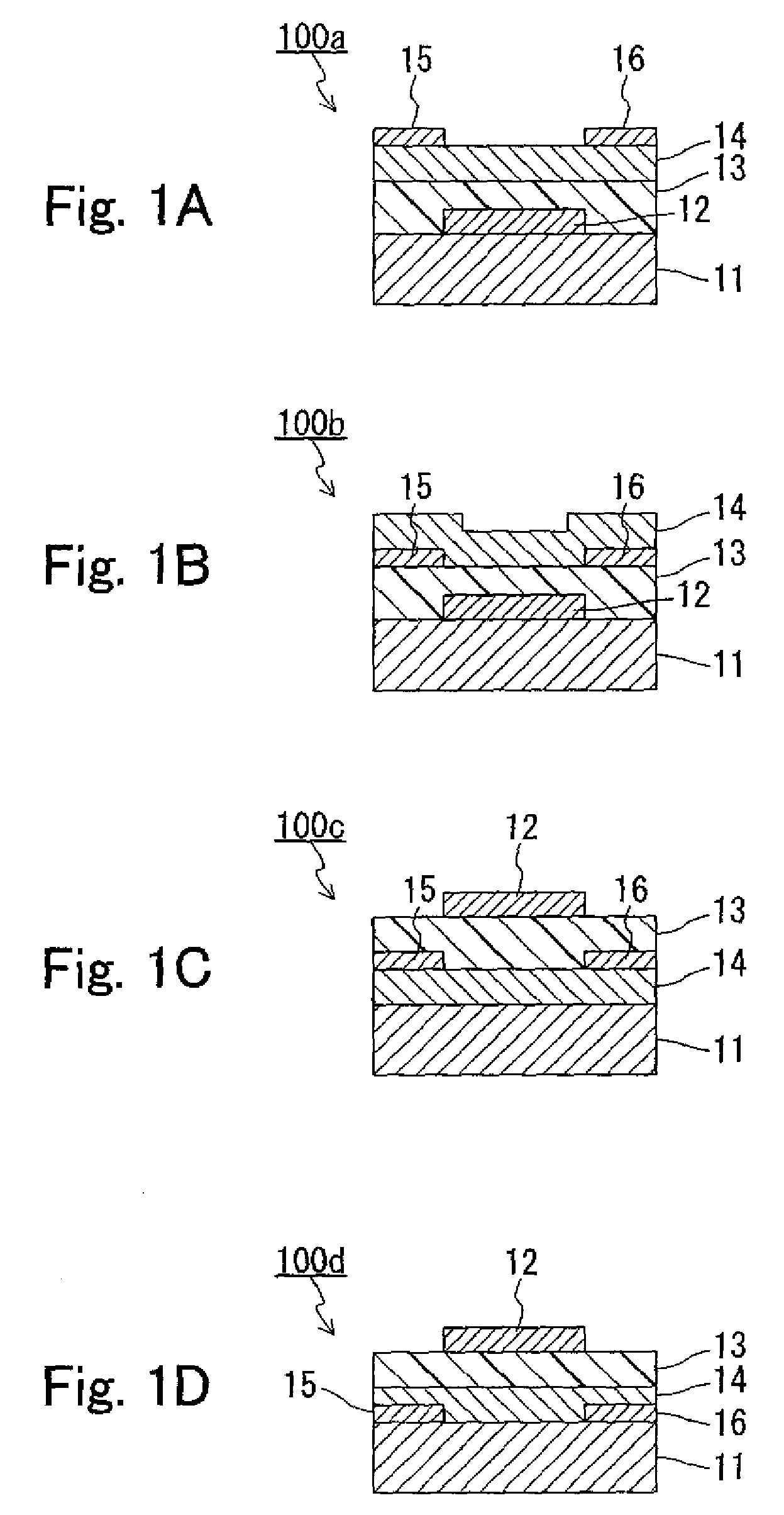
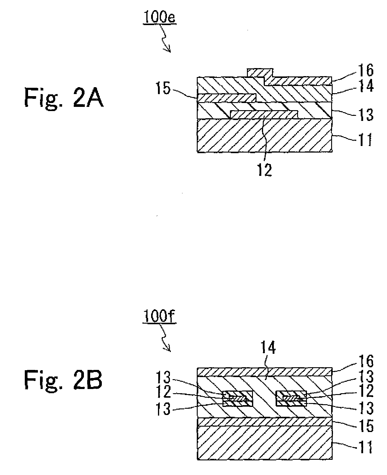
[0092]FIGS. 1A to 1D are cross-sectional views that schematically show a typical example of the TFT of the present invention. As shown in FIGS. 1A to 1D, the TFT of the present invention has various configurations. Any of these TFTs is provided with a substrate 11, a gate electrode 12, a gate insulating layer 13, a semiconductor layer (an organic molecule layer) 14, a source electrode 15, a drain electrode 16 and an electrode modifying layer (not shown). The gate electrode 12 faces the semiconductor layer 14 having the gate insulating layer 13 in between. An electric field applied to the semiconductor layer 14 by the gate electrode 12 controls turning on or off. The electrode modifying layer is composed of the second organic molecules, and the semiconductor layer 14 of the first organic molecules.

[0093]Generally, TFT ...

first example

[0100]An example of manufacturing the TFT 100b shown in FIG. 1B is described as a First Example. In this Example, a polyethylene terephthalate (hereinafter, also referred to as “PET”) film was employed as the substrate 11. The gate electrode 12 was formed by nickel (Ni), and the source and the drain electrodes 15 and 16 were formed by a material that contains gold (Au) as its main component. The organic molecules composing the electrode modifying layers are described later. The gate insulating layer 13 was formed by polyvinyl alcohol. The semiconductor layer 14 was formed by an oligothiophene derivative, which is one of n electron conjugate system molecules.

[0101]FIG. 3A shows the molecular structure of the oligothiophene derivative composing the semiconductor layer 14. FIG. 3B schematically shows the state of a bond and n electron cloud of the oligothiophene derivative. FIG. 3C is a perspective view that schematically shows the π conjugate plane of the oligothiophene derivative wit...

second example

[0119]An example of manufacturing the TFT 100d shown in FIG. 1D is described below. In this Example, the components except the electrode modifying layer were formed by the same materials as the First Example.

[0120]In this example, an electrode modifying layer was formed by the organic molecules shown in FIG. 7A or 7B. Since the source and the drain electrodes were formed by Au in this example as well, disulfide (FIG. 7A) and a compound having mercapto groups (FIG. 7B) were employed for organic molecules through which a tight bond on the Au electrode surface could be expected. The naphthalene portions in the molecule of FIG. 7A and the porphyrin rings in the molecule of FIG. 7B are the main π conjugate planes. In the molecule of FIGS. 7A, S-S linkage is cut and the sulfur atoms and the Au atoms are bonded chemically. In the molecule of FIG. 7B, the sulfur atoms in the mercapto groups and the Au atoms are bonded chemically.

[0121]Hereinafter, the method of manufacturing the TFT 100d in...


PUM

PropertyMeasurementUnit
angleaaaaaaaaaa
angleaaaaaaaaaa
angleaaaaaaaaaa

Abstract

An electronic device of the present invention includes at least one electrode (Au electrode 65) and an organic molecule layer (semiconductor layer 14) formed adjacent to the electrode, and in which charge transfers between the layer and the electrode. The organic molecule layer includes a plurality of first organic molecules containing a conjugated π electron that composes a π conjugate plane (64). A plurality of second organic molecules is bonded chemically to a surface of the electrode at an interface between the electrode and the organic molecule layer. The second organic molecule contains a conjugated π electron that composes a π conjugate plane (67a). The second organic molecule is a molecule having a structure in which the π conjugate plane (67a) and the surface of the electrode form an angle within a predetermined range when the second organic molecule is bonded chemically to the surface of the electrode.

Description

TECHNICAL FIELD[0001]The present invention relates to an electronic device including an organic molecule layer, to a method of manufacturing the same and to an apparatus using the same.BACKGROUND ART[0002]Conventional electronic devices employing inorganic materials use physical properties of bulk materials, typically as crystalline silicon. When the scale of miniaturization reaches the utmost limit, it becomes impossible to obtain the bulk properties and difficult to obtain a desired function. On the other hand, organic materials can assign a function to one molecule and expand them into the device element size, and thereby they can exhibit the desired function.[0003]Organic materials include various compounds having a base of a carbon skeleton. Among them, it was verified that organic molecules with conductivity exhibit diverse electric properties derived from their molecular structures, and proposals have been made for application on various organic electronic devices, such as th...

Claims


Application Information

Patent Timeline
Patent Type & Authority Applications(United States)
IPC IPC(8): H01L51/30
CPCG01N27/414G11C13/0014H01L51/0036H01L51/0051H01L51/0052H01L51/105H01L51/0541H01L51/0545H01L51/0554H01L51/057H01L51/0077H10K85/113H10K85/611H10K85/615H10K85/30H10K10/482H10K10/491H10K10/466H10K10/464H10K10/84
Inventor TAKEUCHI, TAKAYUKIHARADA, KENJIOKUZAWA, TOMOHIROKAMBE, NOBUAKITERAO, JUN
Owner PANASONIC CORP
Why Eureka
Try Eureka