Hybrid Process for Forming Metal Gates of MOS Devices

a technology of metal oxides and mos, applied in the direction of semiconductors, semiconductor devices, electrical devices, etc., can solve the problems of increasing the effective gate dielectric thickness, affecting the efficiency of mos devices, so as to achieve the effect of reducing the threshold voltage of both pmos and nmos devices, and increasing the stress applied to the channel regions of pmos devices

Active Publication Date: 2009-09-17
TAIWAN SEMICON MFG CO LTD
View PDF39 Cites 105 Cited by
  • Summary
  • Abstract
  • Description
  • Claims
  • Application Information

AI Technical Summary

Benefits of technology

[0016]The hybrid method of the present invention provides band-edge work functions for both PMOS and NMOS devices. The stresses applied to the channel regions of PMOS

Problems solved by technology

The depletion effect results in an increase in the effective gate dielectric thickness, making it more difficult for an inversion layer to be created at the surface of the semiconductor.
The use of thin gate dielectrics tends to make the carrier depletion effect worse.
With thin gate dielectrics, the depletion layer in the polysilicon gate becomes more significant in thickness when compared to the thickness of the thin gate dielectrics, and thus device performance degradation worsens.
As a result, the carrier depletion effect in the gate electrodes limits device scalability by imposing a lower bound on how much the effective gate dielectric thickness can be reduced.
However, for PMOS devices, even though metallic materials having band-edge work functions have been found, these materials have poor thermal stability.
The performance of the resulting PMOS devices is thus adversely affected.
Both approaches have advantag

Method used


Image

  • Hybrid Process for Forming Metal Gates of MOS Devices
  • Hybrid Process for Forming Metal Gates of MOS Devices
  • Hybrid Process for Forming Metal Gates of MOS Devices

Examples


Embodiment Construction

[0019]The making and using of the presently preferred embodiments are discussed in detail below. It should be appreciated, however, that the present invention provides many applicable inventive concepts that can be embodied in a wide variety of specific contexts. The specific embodiments discussed are merely illustrative of specific ways to make and use the invention, and do not limit the scope of the invention.

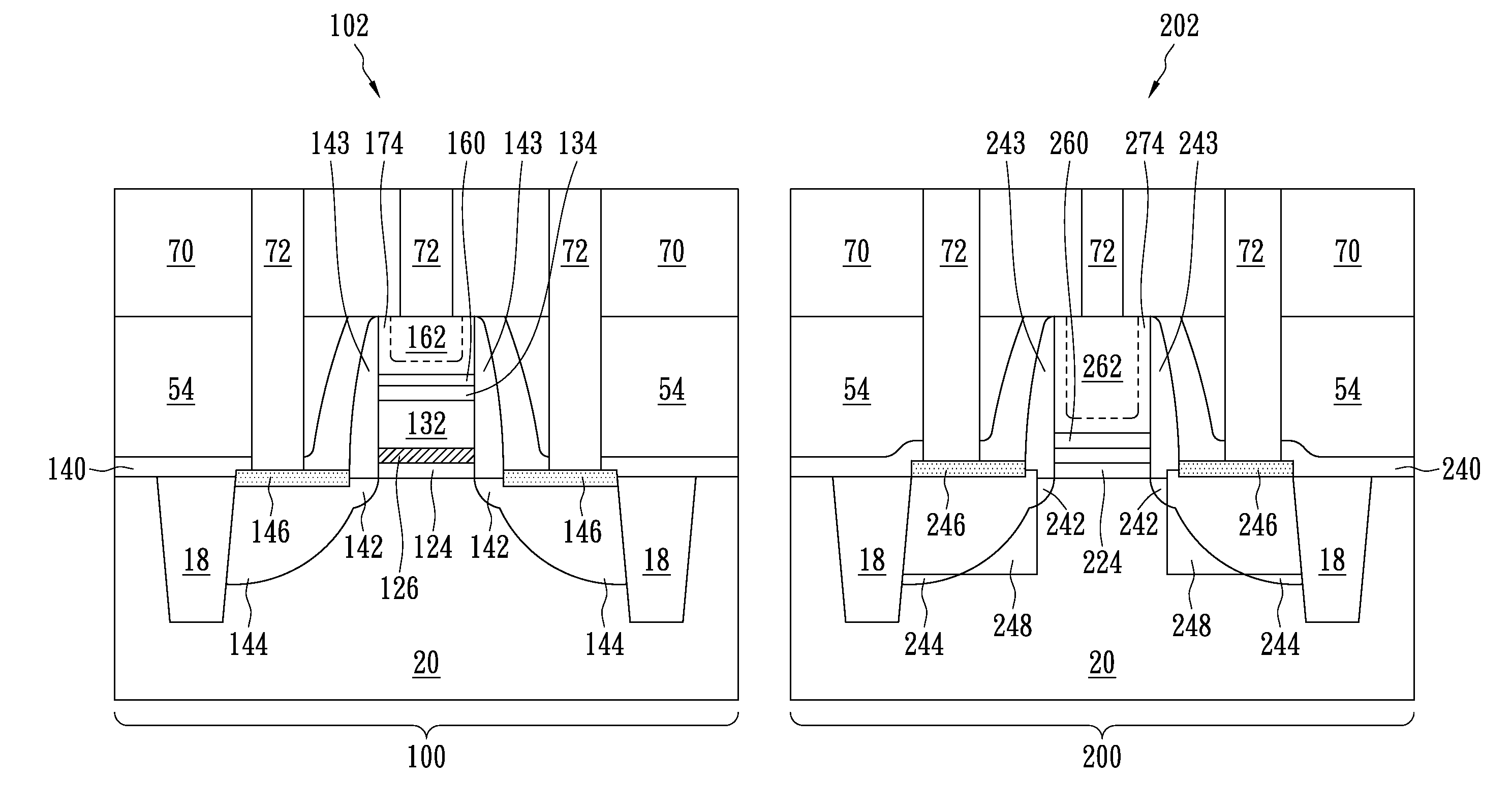
[0020]A method for forming hybrid complementary metal-oxide-semiconductor (CMOS) devices with dual metal gates is provided. The method combines gate-first and gate-last approaches to achieve better effects. The intermediate stages of manufacturing a preferred embodiment of the present invention are illustrated. Throughout the various views and illustrative embodiments of the present invention, like reference numbers are used to designate like elements.

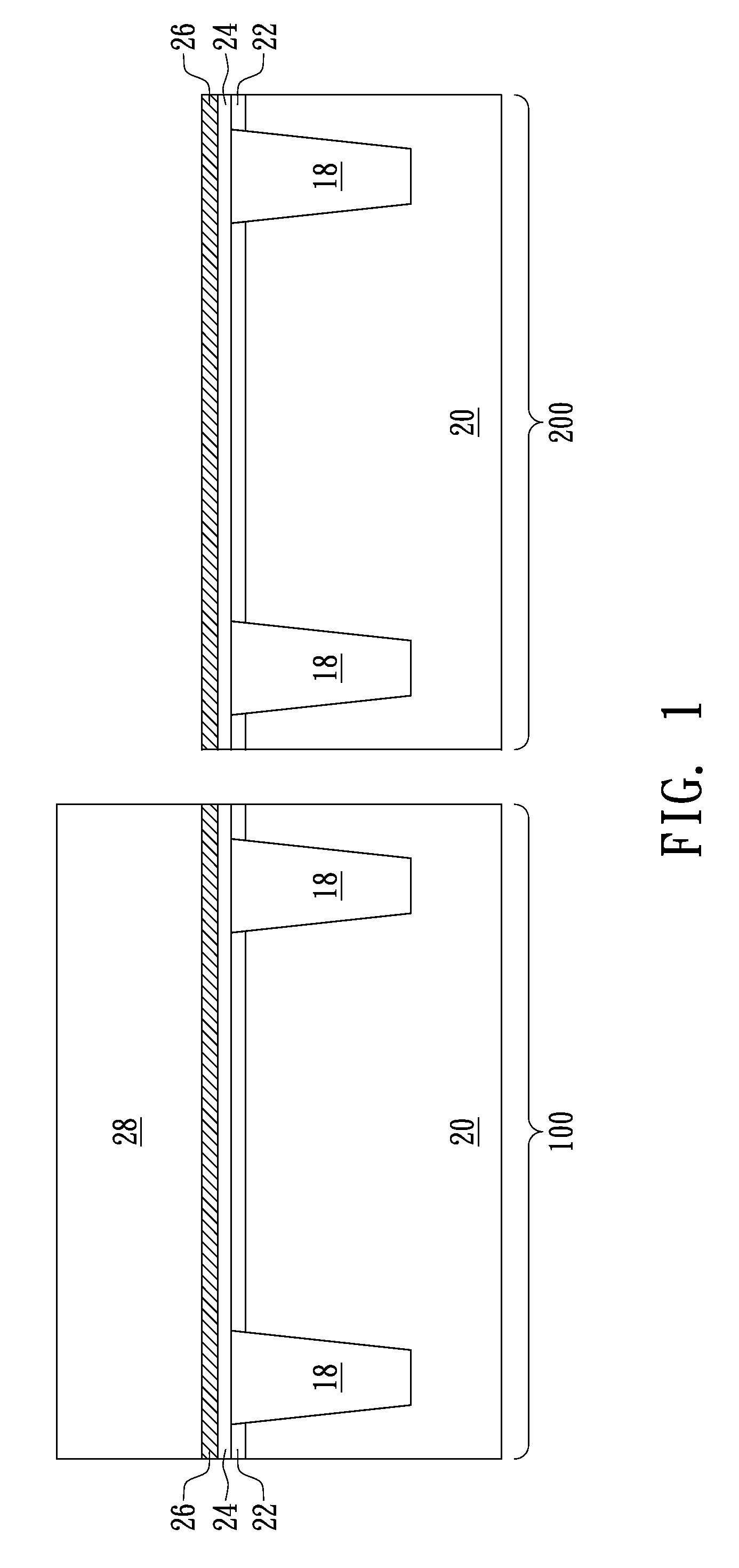
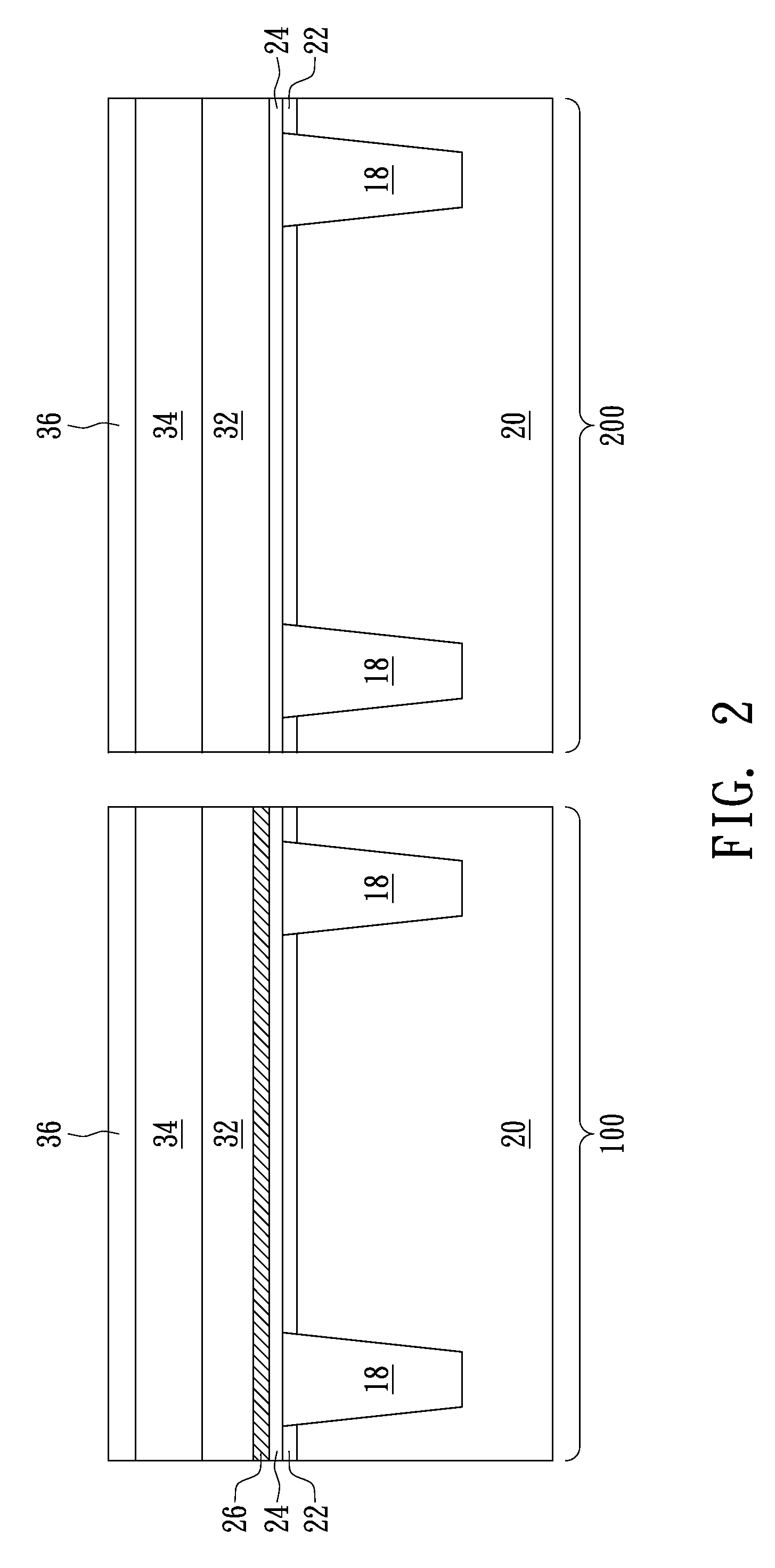
[0021]Referring to FIG. 1, substrate 20 is provided, which may be formed of commonly used semiconductor materials and structur...


PUM


Abstract

A semiconductor structure includes a first MOS device including a first gate, and a second MOS device including a second gate. The first gate includes a first high-k dielectric over a semiconductor substrate; a second high-k dielectric over the first high-k dielectric; a first metal layer over the second high-k dielectric, wherein the first metal layer dominates a work-function of the first MOS device; and a second metal layer over the first metal layer. The second gate includes a third high-k dielectric over the semiconductor substrate, wherein the first and the third high-k dielectrics are formed of same materials, and have substantially a same thickness; a third metal layer over the third high-k dielectric, wherein the third metal layer and the second metal layer are formed of same materials, and have substantially a same thickness; and a fourth metal layer over the third metal layer.

Description

CROSS-REFERENCE TO RELATED APPLICATION[0001]This application relates to the following commonly assigned U.S. patent application: application Ser. No. 11 / 552,704, filed Oct. 25, 2006, entitled “Semiconductor Devices with Dual-Metal Gate Structures and Fabrication Methods Thereof,” which patent application is incorporated herein by reference.TECHNICAL FIELD[0002]This invention relates generally to semiconductor devices, and more particularly to structures of metal-oxide-semiconductor (MOS) devices and manufacturing methods for forming the same.BACKGROUND[0003]Metal-oxide-semiconductor (MOS) devices are basic building elements in integrated circuits. A conventional MOS device typically has a gate electrode comprising polysilicon doped with p-type or n-type impurities, using doping operations such as ion implantation or thermal diffusion. It is preferred to adjust the work function of the gate electrode to the band-edge of the silicon; that is: for an NMOS device, adjusting the work fun...

Claims


Application Information

Patent Timeline
IPC IPC(8): H01L27/092
CPCH01L21/823842H01L27/092H01L21/823857H01L29/7843H01L29/66545H01L29/6659
Inventor HSU, PENG-FUHOU, YONG-TIANLI, SSU-YIHUANG, KUO-TAILIANG, MONG SONG
Owner TAIWAN SEMICON MFG CO LTD
Why Eureka
Try Eureka