Optical semiconductor device

a semiconductor device and optical disc technology, applied in semiconductor devices, diodes, radiation controlled devices, etc., can solve the problems of reduced light receiving sensitivity, increased poor isolation (separation) characteristics between these elements, etc., to increase light receiving sensitivity, reduce leakage current and noise components, and enhance the operating speed of light receiving elements

Inactive Publication Date: 2009-09-17
PANASONIC CORP
View PDF4 Cites 13 Cited by
  • Summary
  • Abstract
  • Description
  • Claims
  • Application Information

AI Technical Summary

Benefits of technology

[0025]In this structure, since the fifth semiconductor layer, which forms a PN junction with the sixth semiconductor layer, is provided in the light absorbing element, part of the first semiconductor layer located in the lower part of the light absorbing element is not depleted. Consequently, carriers generated in part of the light receiving element located in the vicinity of the light absorbing element do not flow into the light absorbing element, thereby enabling the light receiving sensitivity to be increased. Moreover, potential barriers are formed between the fifth semiconductor layer and the first semiconductor layer and between the fifth semiconductor layer and the part of the second semiconductor layer located in the light receiving element, whereby the light receiving element and the light absorbing element are electrically isolated from each other, and leakage current and noise components are reduced. Furthermore, since the light absorbing element does not become a parasitic capacitance component of the light receiving element, the operating speed of the light receiving element is enhanced.

Problems solved by technology

That is, the component that should contribute to the photocurrent is reduced, causing a problem in that the light receiving sensitivity is decreased.
In addition, since the p-type epitaxial layer 106 is a common layer that is also used in the light absorbing element 104 of the photodiode 102, the characteristics of the isolation (separation) between these elements are poor, and leakage current and noise components are increased.
In this case, a problem occurs in that the sensitivity to red or infrared light having a long optical absorption length decreases.
This causes deterioration in the frequency characteristics that depend on the CR product.

Method used


Image

  • Optical semiconductor device
  • Optical semiconductor device
  • Optical semiconductor device

Examples


first embodiment

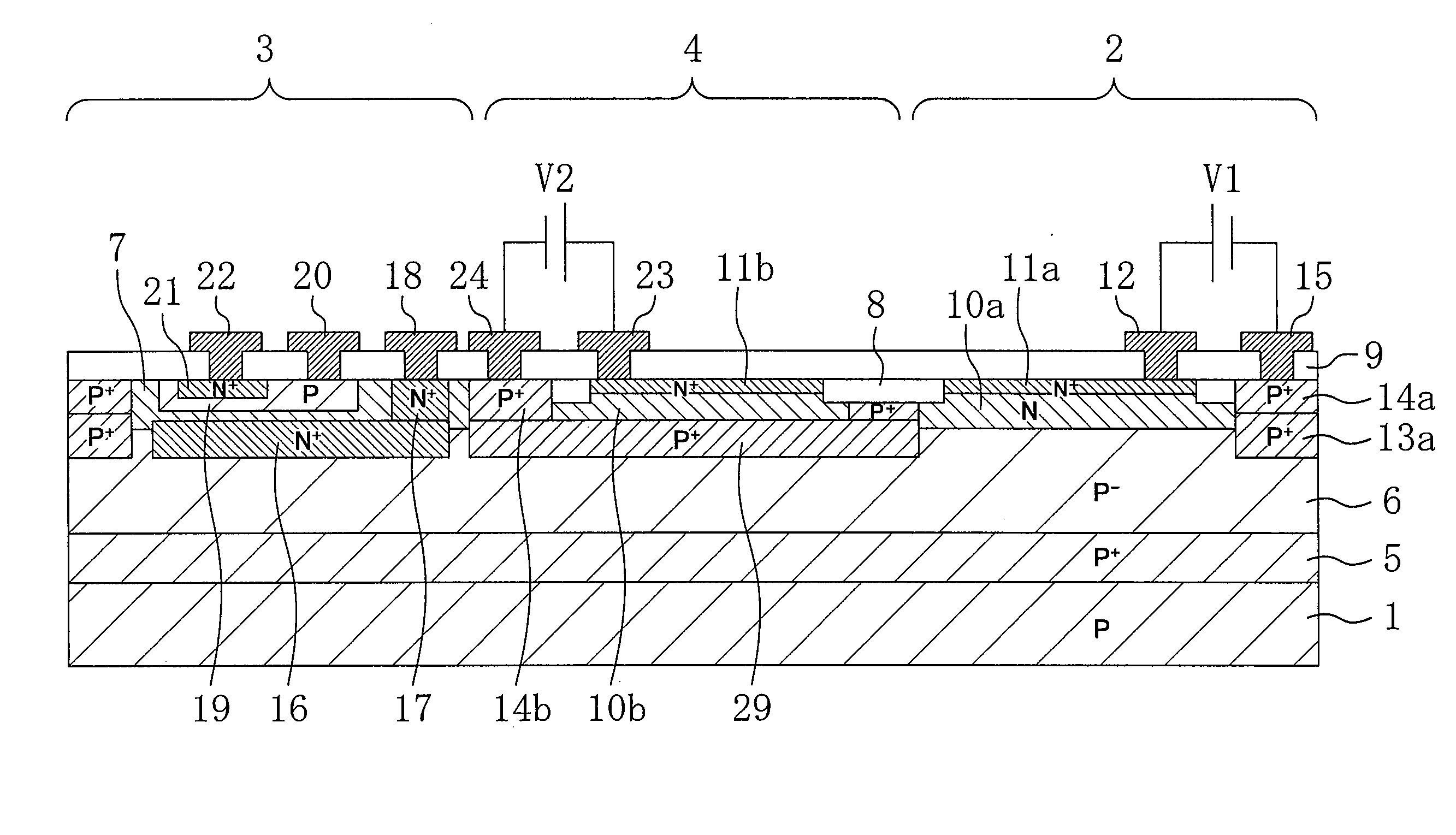
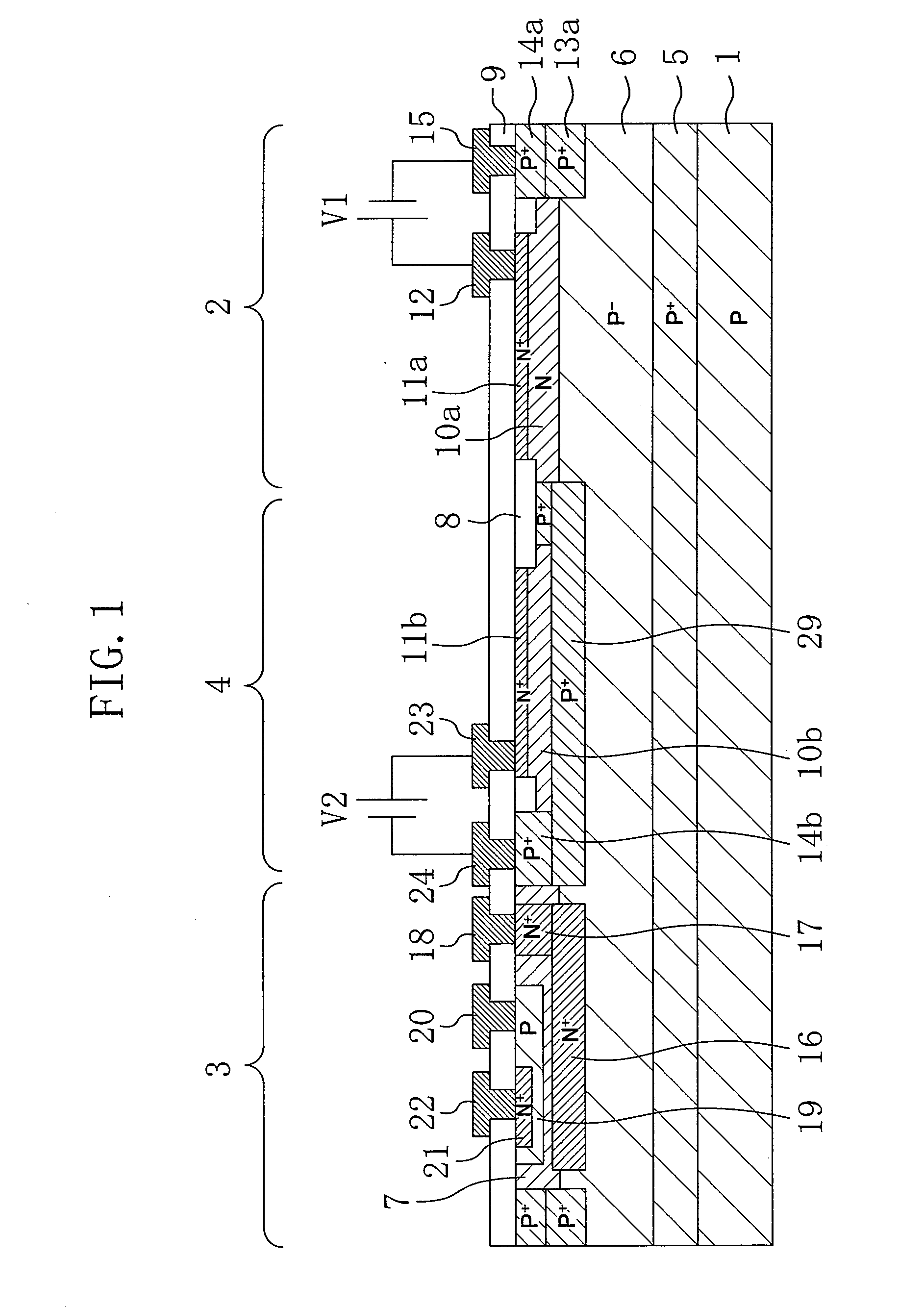
[0034]An optical semiconductor device, which is an OEIC, according to a first embodiment of the present invention will be described below with reference to the accompanying drawings.

[0035]FIG. 1 is a cross-sectional view schematically illustrating the structure of the optical semiconductor device according to the first embodiment. In FIG. 1, the optical semiconductor device in which a pin photodiode as a light receiving element and an NPN transistor as a bipolar transistor (a semiconductor element) are formed on a p-type silicon substrate is illustrated as an example.

[0036]As shown in FIG. 1, the optical semiconductor device according to this embodiment includes: a semiconductor substrate 1 made of silicon, etc. containing a low concentration of a p-type impurity; an NPN transistor 3 formed on the semiconductor substrate 1; a photodiode 2 formed on the semiconductor substrate 1; and a light absorbing element 4 formed in a region on the semiconductor substrate 1 between the NPN trans...

second embodiment

[0057]An optical semiconductor device according to a second embodiment of the present invention will be described below with reference to the accompanying drawings.

[0058]FIG. 5 is a cross-sectional view schematically illustrating the structure of the optical semiconductor device according to the second embodiment. As shown in FIG. 5, the optical semiconductor device of this embodiment is obtained by forming a surface absorption layer 30 on the cathode contact layer 11b in the optical semiconductor device of the first embodiment. In respects other than the surface absorption layer 30, the optical semiconductor device of this embodiment has the same structure as that of the first embodiment.

[0059]The surface absorption layer 30 may be made of a material that can absorb incident light, and it is particularly preferable that the surface absorption layer 30 be made of a material, such as polysilicon or amorphous silicon, for example, that has a larger absorption coefficient for visible l...

third embodiment

[0060]An optical semiconductor device according to a third embodiment of the present invention will be described below with reference to the accompanying drawings.

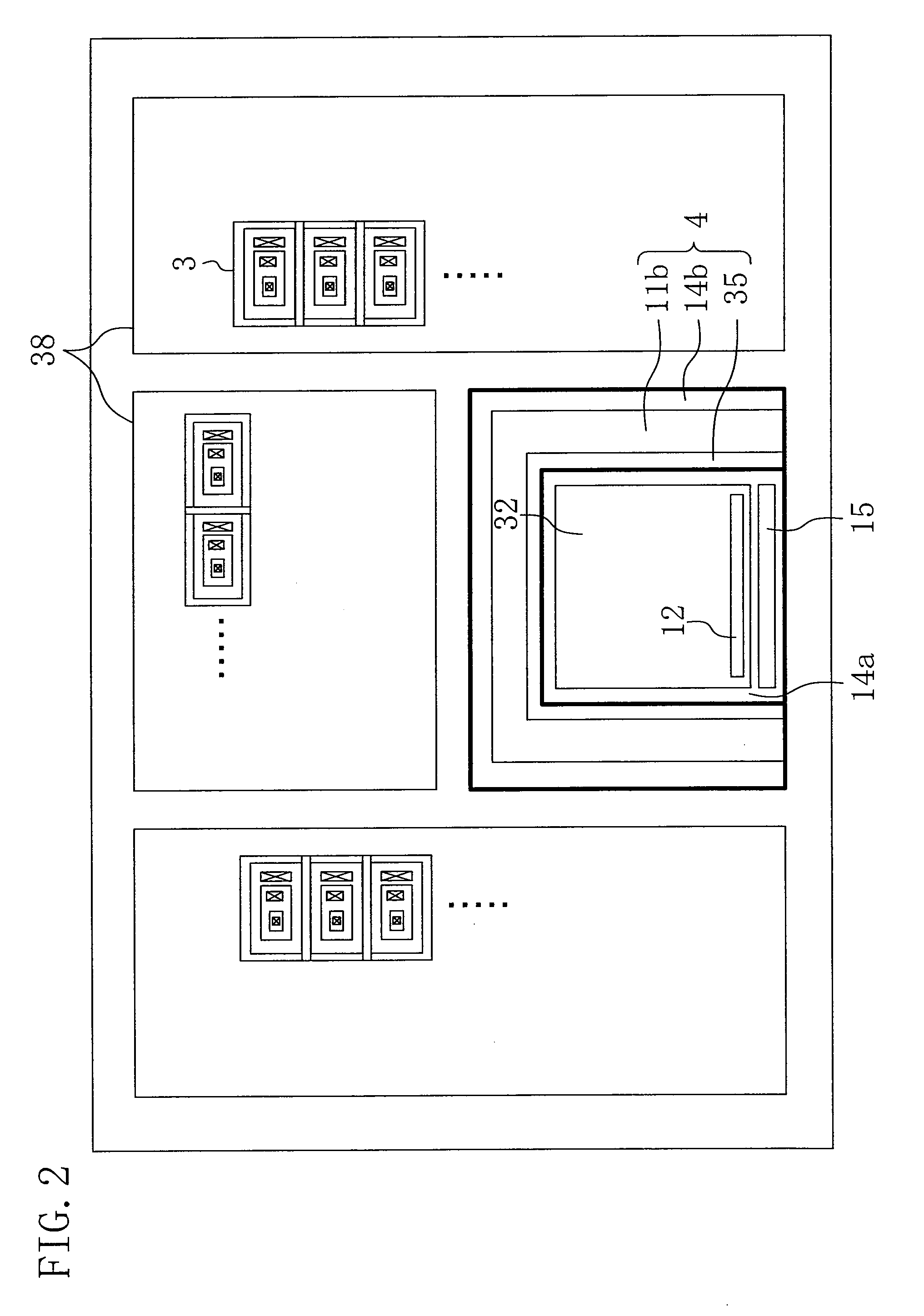
[0061]FIG. 6 is a cross-sectional view schematically illustrating the structure of the optical semiconductor device according to the third embodiment. As shown in FIG. 6, the optical semiconductor device of this embodiment is characterized in that an anode buried layer 13b formed on a p-type epitaxial layer 6 and containing a high concentration of a p-type impurity, an anode contact layer 14c formed on the anode buried layer 13b and containing a high concentration of a p-type impurity, and a third anode electrode 31 formed on the anode contact layer 14c are provided in a region in a photodiode 2 located in the vicinity of a light absorbing element 4. In the other respects, the optical semiconductor device of this embodiment has the same structure as the optical semiconductor device of the first embodiment. FIG. 3 is a plan...


PUM


Abstract

An optical semiconductor device includes a semiconductor substrate; a light receiving element formed on the semiconductor substrate; a light absorbing element formed on the semiconductor substrate and located adjacent to the light receiving element; and a semiconductor element formed on the semiconductor substrate and used for signal processing. The light absorbing element includes a fifth semiconductor layer, and a light absorption region in the light receiving element has a different structure from a light absorption region in the light absorbing element.

Description

CROSS-REFERENCE TO RELATED APPLICATION[0001]This application claims priority from Japanese Patent Application JP2008-062068 filed on Mar. 12, 2008, the disclosure of which application is hereby incorporated by reference into this application in its entirety for all purposes.BACKGROUND OF THE INVENTION[0002]Light receiving elements, which are typical elements of optical semiconductor devices, convert an optical signal to an electrical signal and are used in various fields. In particular, in the field of optical discs, such as CDs (Compact Discs) and DVDs (Digital Versatile Discs), light receiving elements are important as key devices in optical pickup devices that read and write signals recorded on optical discs. In recent years, in response to the demand for higher performance and higher degree of integration, so-called optoelectronic integrated circuits (OEICs), in which a photodiode serving as a light receiving element and various electronic elements, such as a bipolar transistor,...

Claims


Application Information

Patent Timeline
Patent Type & Authority Applications(United States)
IPC IPC(8): H01L31/103
CPCH01L27/1443H01L31/103H01L31/10H01L27/14643
Inventor IWAI, TAKAKITAKEHARA, HIRONARIYASUKAWA, HISATADA
Owner PANASONIC CORP
Why Eureka
Try Eureka