Adhesive Film for Semiconductor and Semiconductor Device Therewith
a technology for adhesive films and semiconductors, applied in the direction of film/foil adhesives without carriers, film/foil adhesives, adhesive types, etc., can solve the problems of low reliability and tendency to form cracks, and achieve the effect of reducing the melting temperatur
- Summary
- Abstract
- Description
- Claims
- Application Information
AI Technical Summary
Benefits of technology
Problems solved by technology
Method used
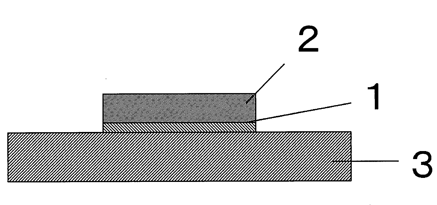
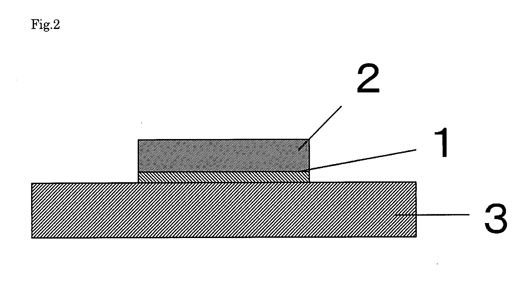
Image

Examples
example 1
(1) Preparation of a Varnish of an Adhesive Film for a Semiconductor Resin
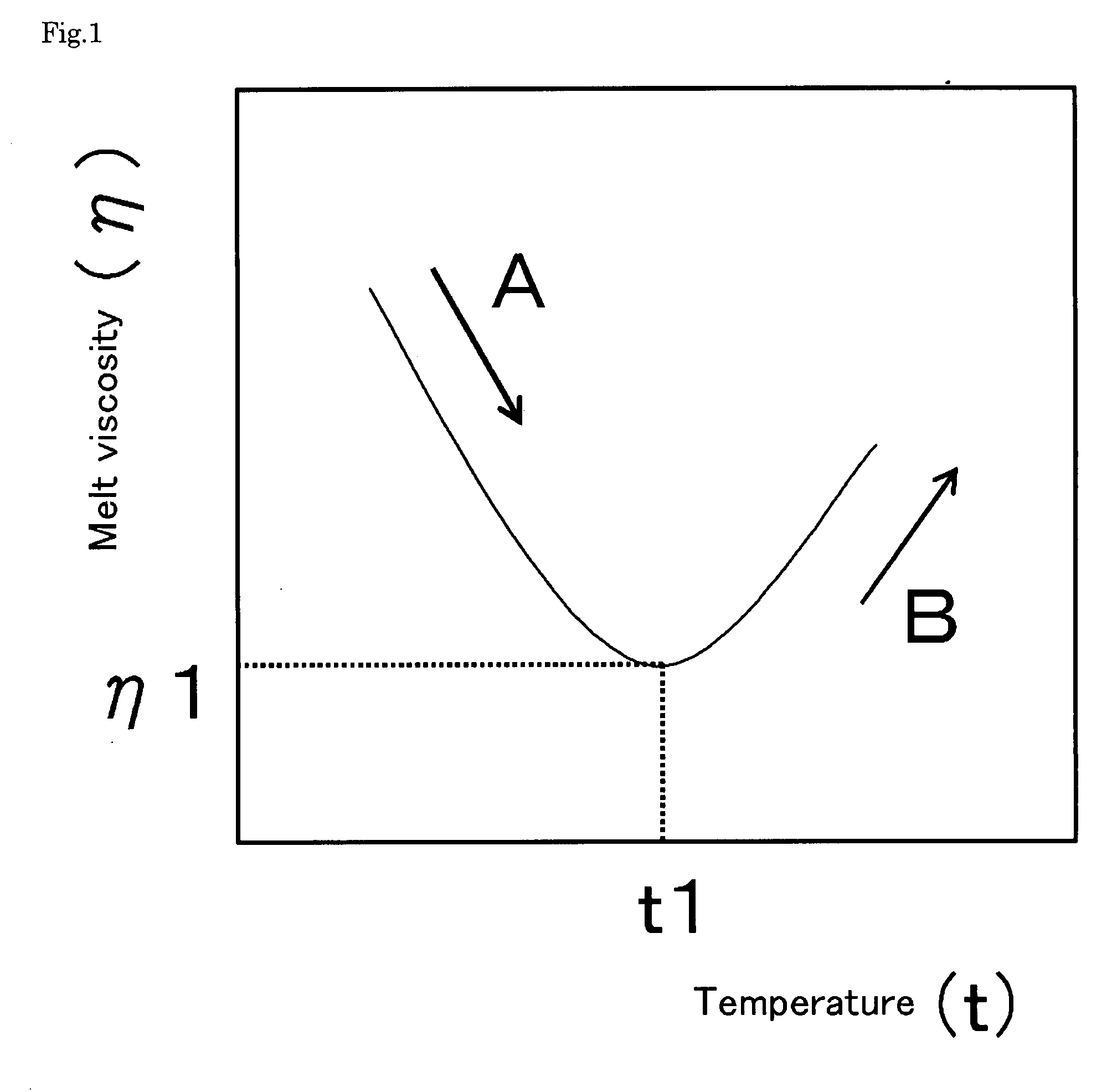
[0056]In methyl ethyl ketone (MEK) were dissolved 100 parts by weight of an acrylate copolymer (butyl acrylate-acrylonitrile-ethyl acrylate-glycidyl methacrylate copolymer, Nagase ChemteX Corp., SG-80HDR, Tg: 10° C., weight-average molecular weight: 350,000) as a thermoplastic resin (A), 97 parts by weight of epoxy resin (EOCN-1020-80 (ortho-cresol novolac type epoxy resin), epoxy equivalent 200 g / eq, Nippon Kayaku Co., Ltd.) as a hardening resin, 146 parts by weight of NC6000 (epoxy equivalent 200 g / eq, Nippon Kayaku Co., Ltd.), 110 parts by weight of a liquid phenol compound (MEH-8000H, hydroxy equivalent 141 g / OH group, Meiwa Plastic Industries, Ltd.), 47 parts by weight of a solid phenol resin (PR-HF-3, hydroxy equivalent 104 g / OH group, Sumitomo Bakelite Co., Ltd.), 0.75 parts by weight of an imidazole compound (2P4 MHZ-PW, Shikoku Chemicals Corp.) as a curing accelerator and 1.3 parts by weight of γ-glyc...
example 2
[0082]An experiment was conducted as described in Example 1, except using 99 parts by weight of EOCN-1020-80 (epoxy equivalent 200 g / eq, Nippon Kayaku Co., Ltd.) as an epoxy resin, 148 parts by weight of NC6000 (epoxy equivalent 200 g / eq, Nippon Kayaku Co., Ltd.), 92 parts by weight of MEH-8000H (hydroxy equivalent 141 g / OH group, Meiwa Plastic Industries, Ltd.) as a liquid phenol compound (C) and 62 parts by weight of PR-HF-3 (hydroxy equivalent 104 g / OH group, Sumitomo Bakelite Co., Ltd.) as a solid phenol resin. Table 1 shows the composition and the experimental results.
example 3
[0083]An experiment was conducted as described in Example 1, except using 110 parts by weight of MEH-8000-4L (hydroxy equivalent 141 g / OH group, Meiwa Plastic Industries, Ltd.) as a liquid phenol compound (C). Table 1 shows the composition and the experimental results.
PUM
| Property | Measurement | Unit |
|---|---|---|
| temperature | aaaaa | aaaaa |
| melt viscosity | aaaaa | aaaaa |
| die shear strength | aaaaa | aaaaa |
Abstract
Description
Claims
Application Information
 - R&D
- Intellectual Property
- Life Sciences
- Materials
- Tech Scout
- Unparalleled Data Quality
- Higher Quality Content
- 60% Fewer Hallucinations
Browse by: Latest US Patents, China's latest patents, Technical Efficacy Thesaurus, Application Domain, Technology Topic, Popular Technical Reports.
© 2025 PatSnap. All rights reserved.Legal|Privacy policy|Modern Slavery Act Transparency Statement|Sitemap|About US| Contact US: help@patsnap.com