Photoactive device with organic layers

a photoactive device and organic technology, applied in the field of organic photoactive devices, can solve the problems of deteriorating the transport properties of charge carriers in comparison to pure layers, inability to use monocrystalline organic materials, and difficult production of multiple layers with sufficient structural perfection

Inactive Publication Date: 2009-09-24
HELIATEK GMBH +1
View PDF1 Cites 70 Cited by
  • Summary
  • Abstract
  • Description
  • Claims
  • Application Information

AI Technical Summary

Benefits of technology

[0055]A purposeful embodiment of the invention can provide that a lowest unoccupied molecular orbital (LUMO) of the organic material (B) is energetically lower or at the most approximately 0.1 eV higher than the lowest unoccupied molecular orbital (LUMO) of the organic material (A).
[0056]An advantageous embodiment of the invention provides that a highest occupied molecular orbital (HOMO) of the at least one further organic material (B) is energetically higher or at the most approximately 0.1 eV lower than the highest occupied molecular orbital (HOMO) of the organic material (A).

Problems solved by technology

However, for large-area applications the use of monocrystalline organic materials is not possible and the production of multiple layers with sufficient structural perfection has been very difficult up to now.
Moreover, since each of the individual materials only fill out a part of the mixed layer, the transport properties for the charge carriers clearly deteriorate in comparison to the pure layers.
However, the direct use of such materials with elevated ISC probability as component of an organic heterojunction entails various problems.
The excitation energy then relaxes very quickly into the lowest state, which means an energy loss for the solar cell.

Method used


Image

  • Photoactive device with organic layers
  • Photoactive device with organic layers
  • Photoactive device with organic layers

Examples


first exemplary embodiment

[0095]The following layer sequence is provided in a first exemplary embodiment: ITO / DCV3T*C60 / MeOTPD / p-doped MeOTPD / gold. ITO designates a transparent ground contact here of indium-tin oxide and C60 the Buckminster fullerene.

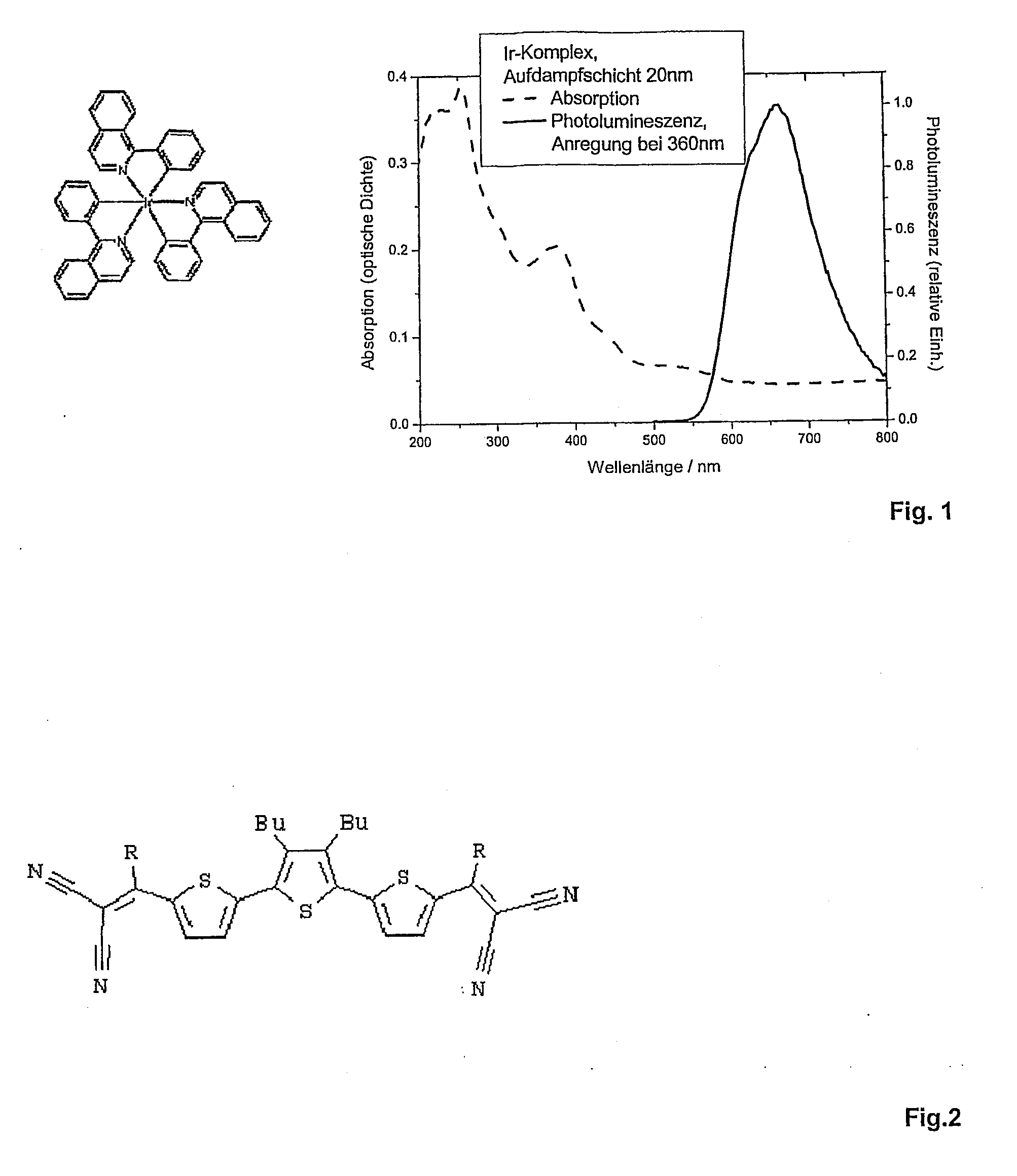
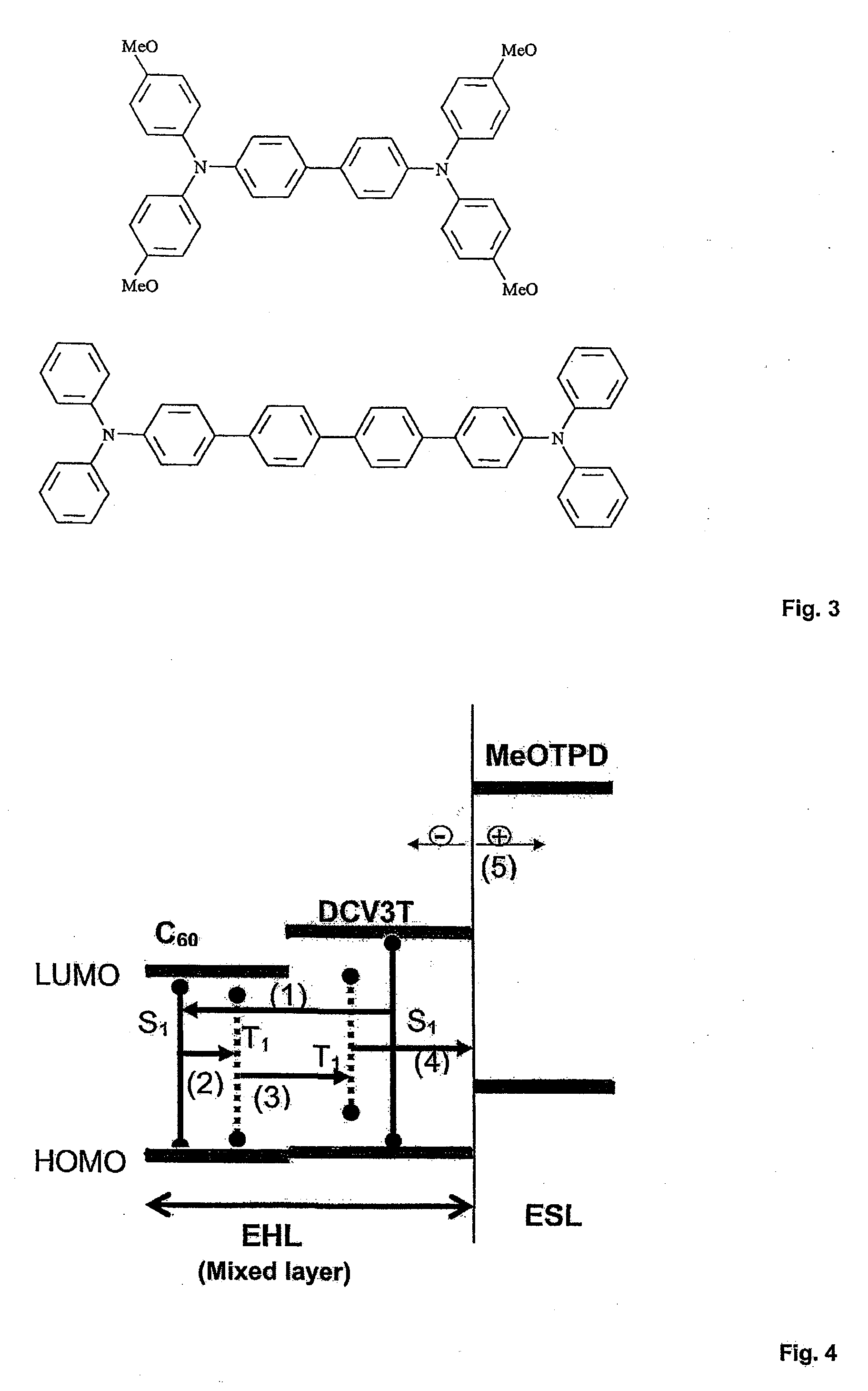
[0096]The structure of the other materials is shown in FIG. 2 and FIG. 3. FIG. 2 shows the structural formula of DCV3T. The group R in DCV3T is a hydrogen atom but can also be a cyano group (TCV3T, cf. T. M. Pappenfus et al., Org. Lett. 5 (9), 1535-1538 (2003)) or an alkyl group in derivatives. FIG. 3 shows the chemical structure of MeOTPD (above in FIG. 3; MeO designates a methoxy group) and 4P-TPD (below in FIG. 3).

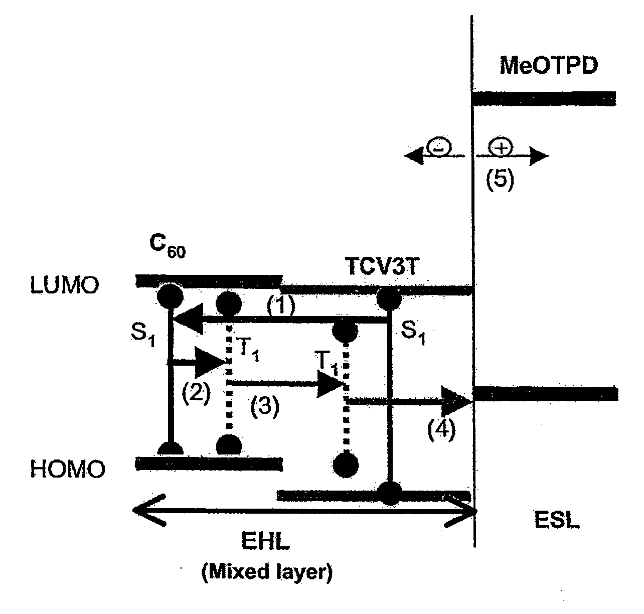
[0097]The p-doping takes place e.g., by mixed vapor deposition with perfluorinated tetracyano quinodimethane (F4-TCNQ). In this first exemplary embodiment the exciton-harvesting layer consists of DCV3T (organic material A) and C60 (further organic material B) and the exciton-separating layer of MeOTPD.

[0098]FIG. 4 shows a schematic representation fo...

second exemplary embodiment

[0108]In a second exemplary embodiment the following layer sequence is provided for the photoactive device: ITO / C60 / DCV3T*C60 / MeOTPD / p-doped MeOTPD / gold.

[0109]In distinction to the first exemplary embodiment an additional pure C60 layer is arranged here as a triplet blocking layer (TBL) between the exciton-harvesting layer and the ITO electrode. The method of functioning of the device corresponds to that of the device in accordance with the first exemplary embodiment. The triplet blocking layer fulfils the function of preventing triplet excitons that diffuse in the direction of the ITO electrode from being quenched there. Instead, the triplet excitons are reflected on C60 and have another chance to reach the interface to the exciton-harvesting layer. FIG. 7 shows a current-voltage characteristics under illumination with simulated sunlight with an intensity of 127 mW / cm2 and without illumination for a device in accordance with the second exemplary embodiment with a 30 nm-thick mixed ...

third exemplary embodiment

[0110]In a third exemplary embodiment the following layer sequence is provided for the photoactive device: ITO / C60 / DCV3T*C60 / DCV3T / MeOTPD / p-doped MeOTPD / gold.

[0111]In distinction to the second exemplary embodiment an additional pure layer (TTL—triplet transport layer) of DCV3T (organic material A of the exciton-harvesting layer) is introduced between the exciton-harvesting layer and the exciton-separating layer. The triplet excitons, that are formed in the exciton-harvesting layer, must additionally diffuse here through the DCV3T layer until they can be separated at the interface to the exciton-separating layer into holes on MeOTPD and electrons on DCV3T.

[0112]The fact that the transfer of triplet excitons takes place from C60 onto DCV3T and the diffusion of the transferred triplet excitons onto DCV3T is proven by the signal clearly coming from C60 in the external quantum efficiency of a solar cell with the layer sequence ITO / C60 / DCV3T / MeOTPD / p-doped MeOTPD / gold (cf. FIG. 8). In the...


PUM

PropertyMeasurementUnit
LUMOaaaaaaaaaa
HOMOaaaaaaaaaa
energyaaaaaaaaaa

Abstract

The invention relates to a photoactive device with organic layers, especially a solar cell, with a layer arrangement having an electrode and a counterelectrode as well as a sequence of organic layers arranged between the electrode and the counterelectrode, wherein two layers bordering on one another are formed in a photoactive region encompassed by the sequence of organic layers, namely, an exciton-harvesting layer (EHL) and an exciton-separating layer (ESL); in which the exciton-harvesting layer (EHL) is a mixed layer containing an organic material (A) and at least one further organic material (B), in which (i) a lowest singlet excitation state for excitons (S1A) of the organic material (A) is energetically higher than a lowest singlet excitation state for excitons (S1B) of the further organic material (B), (ii) the further organic material (B) is chosen such that it transforms singlet excitons into triplet excitons with a quantum yield of at least approximately 20%, preferably of at least approximately 50% by an ISC mechanism (ISC—Inter-System-Crossing), and (iii) a lowest triplet excitation state for excitons (T1B) of the further organic material (B) is energetically higher than a lowest triplet excitation state for excitons (T1A) of the organic material (A); and wherein a donor-acceptor heterojunction is formed between the exciton-harvesting layer (EHL) and the exciton-separating layer (ESL) converting triplet excitons of the organic material (A) into free charge carrier pairs in the vicinity of the interface.

Description

CROSS REFERENCE TO RELATED APPLICATIONS[0001]This is a continuation of U.S. patent application Ser. No. 11 / 817,636, filed Aug. 31, 2007, in the name of Martin PFEIFFER, Christian UHRICH, Annette PETRICH, Rico SCHÜPPEL, Karl LEO, Peter BÄUERLE, Eduard BRIER, and Pinar KILICKIRAN and entitled PHOTOACTIVE DEVICE WITH ORGANIC LAYERS, which was the National Stage of International Application No. PCT / DE2006 / 000409, filed 3 Mar. 2006, which claims priority of German Patent Application No. 10 2005 010 979.9, filed Mar. 4, 2005, which are herein incorporated by reference. The PCT International Application was published in the German Language.[0002]The invention relates to a photoactive device with organic layers, especially a solar cell, with a layer arrangement having an electrode and a counterelectrode as well as a sequence of organic layers arranged between the electrode and the counterelectrode.BACKGROUND OF THE INVENTION[0003]Since the demonstration of the first organic solar cell with ...

Claims


Application Information

Patent Timeline
Patent Type & Authority Applications(United States)
IPC IPC(8): H01L31/042H01L31/00H01L31/18B82B1/00
CPCB82Y10/00H01L51/0036H01L51/0046H01L51/0047H01L51/0048Y02E10/549H01L51/0077H01L51/0078H01L51/0085H01L51/4246H01L51/4253H01L51/0053H10K85/113H10K85/211H10K85/215H10K85/221H10K85/621H10K85/311H10K85/30H10K85/342H10K30/211H10K30/30
Inventor PFEIFFER, MARTINUHRICH, CHRISTIANPETRICH, ANNETTESCHUPPEL, RICOLEO, KARLBAUERLE, PETERBRIER, EDUARDKILICKIRAN, PINAR
Owner HELIATEK GMBH
Why Eureka
Try Eureka