Method of manufacturing semiconductor device for providing improved isolation between contact and cell gate electrode

a technology of semiconductor memory and contact, which is applied in the direction of semiconductor memory devices, basic electric elements, electrical appliances, etc., can solve the problems of reducing the dimension of the semiconductor memory cell, reducing the gate length below the quarter micron order, and avoiding short-circuiting

Inactive Publication Date: 2009-09-24
RENESAS ELECTRONICS CORP
View PDF3 Cites 6 Cited by
  • Summary
  • Abstract
  • Description
  • Claims
  • Application Information

AI Technical Summary

Benefits of technology

[0021]The present invention effectively avoids short-circuiting between a bitline and a cell gate electrode and / or short-circuiting between a capacitor electrode and a cell gate electrode.

Problems solved by technology

The dimension reduction in the semiconductor memory cell is, however, undesirably accompanied by the difficulty in providing a clearance between the gate electrode and the cell contact within each memory cell.
One issue in next generation semiconductor devices in which the gate length is reduced below the quarter micron order is production of minute particles during the gate electrode formation.
Minute particles may work as etching masks and cause production of skirt-like etching residuals adjacent to the gate electrodes.
The skirt-like etching residuals may be directly contacted to the cell contacts formed thereafter, causing short-circuiting between a bitline and a gate electrode or between a capacity electrode and the gate electrode.
This may undesirably lower the production yield.
It is also a problem that the defects resulting from the minute particles necessitate performing product screening for detecting initial defects with severe conditions.
One currently-used approach to address this problem is optimization of the etching conditions for reducing minute particles; however, further advance is desired to address the problem of minute particles, since the detection by an automatic defect detecting machine may face limitations with the further dimension reduction.

Method used


Image

  • Method of manufacturing semiconductor device for providing improved isolation between contact and cell gate electrode
  • Method of manufacturing semiconductor device for providing improved isolation between contact and cell gate electrode
  • Method of manufacturing semiconductor device for providing improved isolation between contact and cell gate electrode

Examples


first embodiment

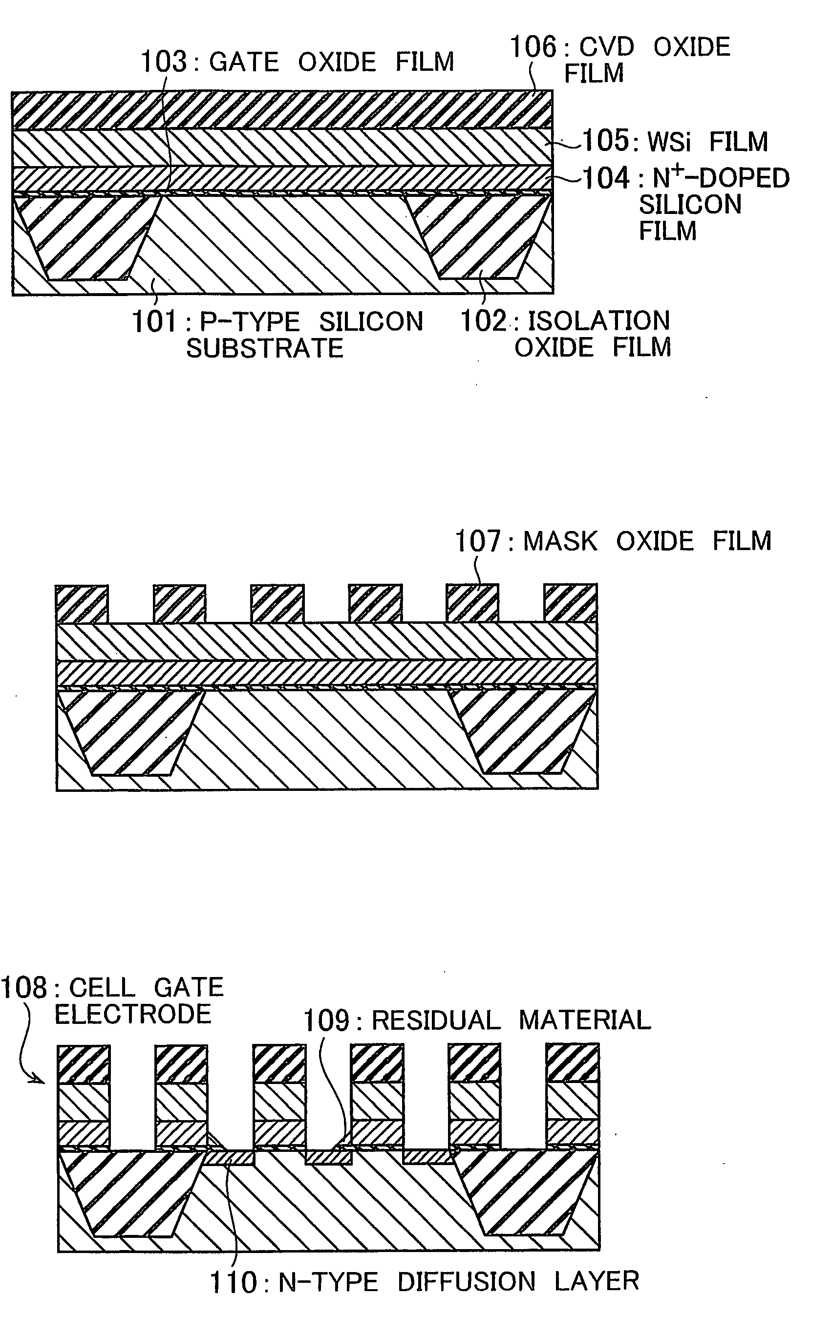
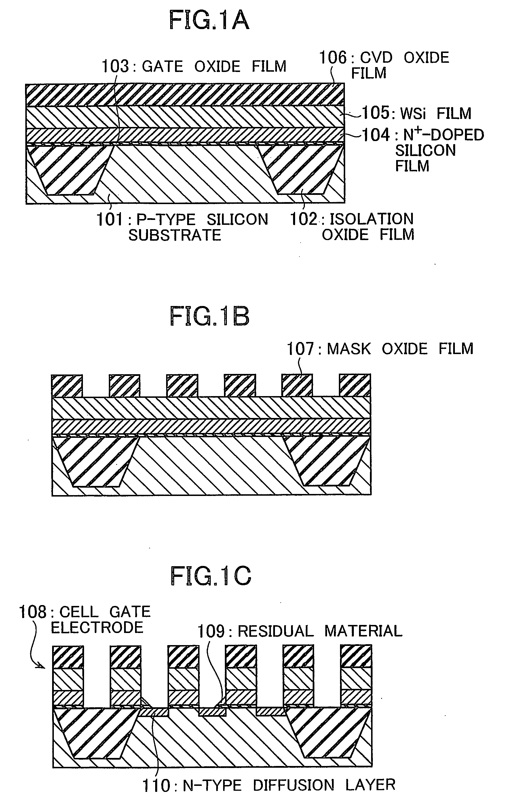
[0027]Referring to FIGS. 2A to 2K, a description is given below of an exemplary process of manufacturing a semiconductor device in a first embodiment of the present invention. The manufacture process of this embodiment begins with forming isolation oxide films 2 with a depth of 0.25 to 0.40 μm on the surface of a P-type silicon substrate 1 by using a trench isolation technique. Gate oxide films 3 are then formed with a thickness of 5 to 10 nm in respective active regions isolated by the isolation oxide films 2. This is followed by sequentially forming an N+-doped silicon film 4 with a thickness of 0.1 to 0.15 μm, a tungsten silicide film 5 with a thickness of 0.1 to 0.15 μm, and a CVD oxide film 6 with a thickness of 0.2 to 0.3 μm to cover the P-type silicon substrate 1, as shown in FIG. 2A.

[0028]Subsequently, mask oxide films 7 with a width of 0.11 to 0.2 μm are formed by etching the CVD oxide film 6 with a photoresist pattern used as a mask, as shown in FIG. 2B. Furthermore, cell ...

second embodiment

[0033]A description is then given of an exemplary process of manufacturing a semiconductor device in a second embodiment of the present invention, referring to FIGS. 3A to 3K. The first embodiment is directed to provide a solution to the problem that the local residuals 9 formed of N+-doped silicon due to the formation of the minute particles of 0.05 to 0.15 μm working as a mask in the etching process of the N+-doped silicon film 4.

[0034]On the other hand, the second embodiment is directed to avoid a problem caused by minute particles of 0.05 to 0.15 μm produced in etching the CVD oxide film 6 with a photoresist pattern used as a mask.

[0035]As shown in FIG. 3A, the process of the second embodiment begins with forming the isolation oxide films 2, the gate oxide films 3, the N+-doped silicon film 4, the tungsten silicide film 5, and the CVD oxide film 6 in the same manner as that of the first embodiment. This is followed by forming the mask oxide films 7 by etching the CVD oxide film ...


PUM


Abstract

A manufacture method is provided for forming a semiconductor device. The method includes: forming a plurality of gate electrodes through etching a conductive film deposited on a semiconductor substrate; forming a first nitride film to cover the gate electrodes; partially exposing the semiconductor substrate in a region between adjacent two of the gate electrodes through performing an etch-back process on the first nitride film; thermally oxidizing a residual of the gate electrode film remaining in the region between the adjacent two of the gate electrodes to change the residual into an thermal oxide film; and forming a contact in the region between the adjacent two of the gate electrodes.

Description

INCORPORATION BY REFERENCE [0001]This application claims the benefit of priority based on Japanese Patent Application No. 2008-076054, filed on Mar. 24, 2008, the disclosure of which is incorporated herein by reference.BACKGROUND OF THE INVENTION [0002]1. Field of the Invention[0003]The present invention relates to a method for manufacturing a semiconductor device, more particularly, to a technique for forming memory cell contacts of a semiconductor memory device such as a DRAM (dynamic random access memory) and a pseudo SRAM (static random access memory).[0004]2. Description of the Related Art[0005]Recently, dimension reduction has been advanced in memory devices, such as DRAMs, which include one transistor and one capacitor in each memory cell, and pseudo SRAMs, which have the same cell structure as that of DRAMs. The dimension reduction provides an increased memory capacity while reducing the chip cost due to the yield increase.[0006]The dimension reduction in the semiconductor m...

Claims


Application Information

Patent Timeline
Patent Type & Authority Applications(United States)
IPC IPC(8): H01L29/43H01L21/302
CPCH01L21/28247H01L21/76831H01L27/10888H01L27/10855H01L27/10873H01L21/76897H10B12/05H10B12/485H10B12/0335H01L21/82H01L21/28H01L21/18
Inventor TASAKA, KAZUHIRO
Owner RENESAS ELECTRONICS CORP
Why Eureka
Try Eureka