Semiconductor memory device and operation method therefor
Inactive Publication Date: 2009-09-24
SONY CORP
View PDF8 Cites 15 Cited by
Summary
Abstract
Description
Claims
Application Information
AI Technical Summary
This helps you quickly interpret patents by identifying the three key elements:
Problems solved by technology
Method used
Benefits of technology
Benefits of technology
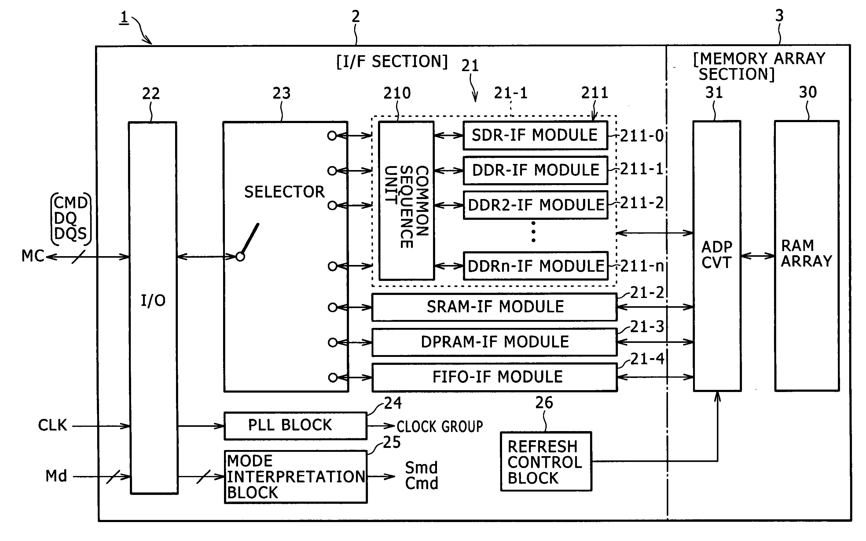
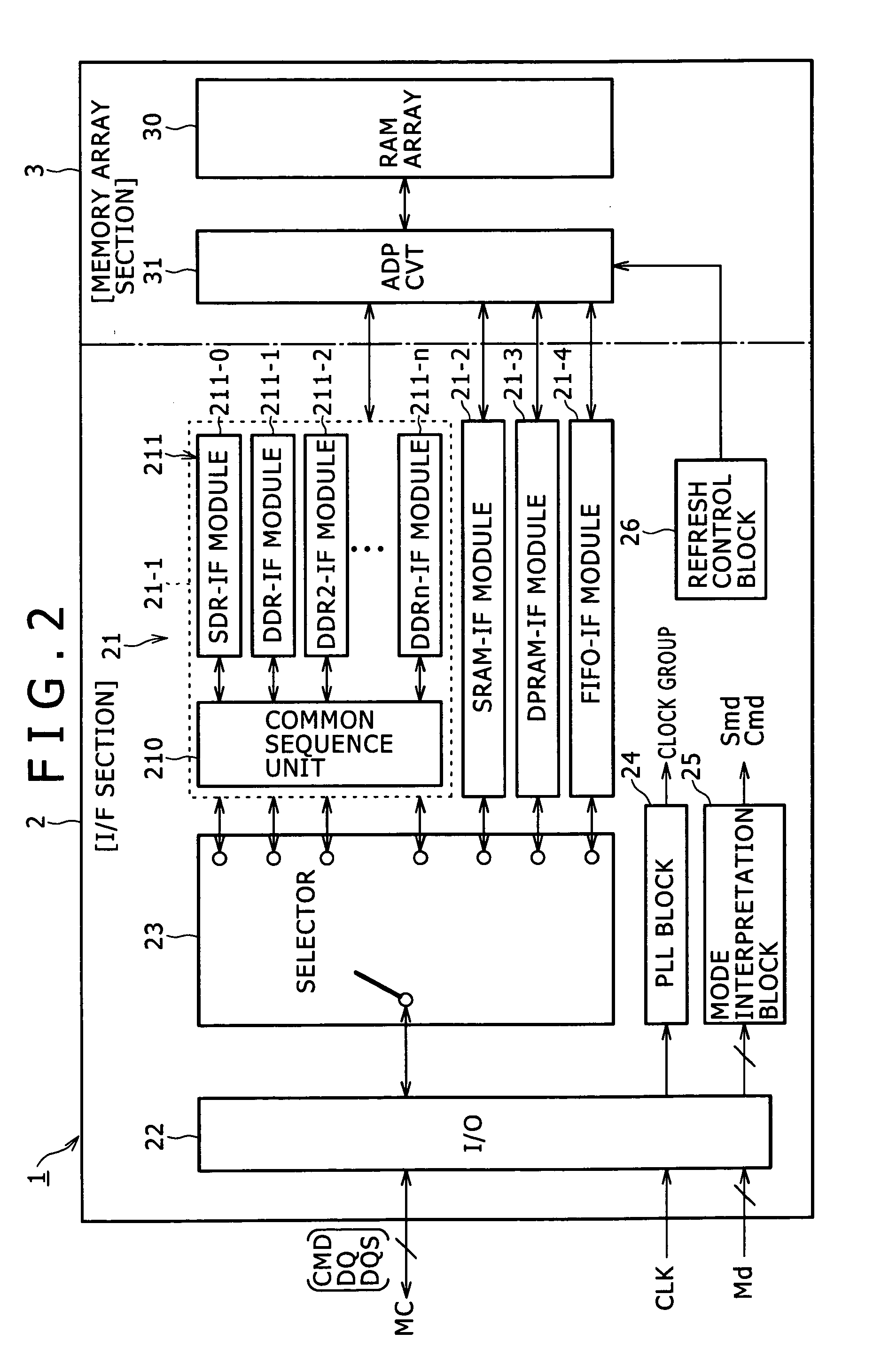
[0028]Preferably, the refresh control block further has a function of skipping the refresh command to an address of the memory array which has been accessed within the refresh cycle thereby eliminate the necessity for the refreshment.
[0034]According to another embodiment of the present invention, there is provided an operation method for a semiconductor memory device having an interface function in accordance with a memory type between a memory array section wherein a memory array which requires a refresh operation is formed and an external apparatus, including the steps of issuing a refresh command within a refresh cycle, and skipping, if an access command and the refresh command to the memory array collide with each other, the refresh command for any address of the memory array accessed within the refresh cycle to eliminate the necessity for the refreshment for the address.
[0036]With the semiconductor memory device and the operation method therefor, the semiconductor memory device can be used as memories of various memory types, and besides can carry out a refresh operation in response to an access situation. Consequently, efficient memory accessing can be achieved.
[0037]Further, the semiconductor memory device can be used to achieve improvement in efficiency in apparatus fabrication and design and stabilization in fabrication.
[0038]For example, if supply of a memory of a certain memory type for use in an electronic apparatus which incorporates a memory of the memory type becomes unstable, then if the memory is replaced by the semiconductor memory device and the semiconductor memory device is set so that it executes operation similar to that of the memory formerly used, then fabrication of the apparatus can be continued without changing the design of a memory control circuit or peripheral circuits.
[0039]Further, where a new electronic apparatus is to be designed, if the semiconductor memory device is adopted as a memory chip to be incorporated in the electronic apparatus, then the electronic apparatus can be designed efficiently with a high degree of freedom. Also in a case wherein it is intended to carry out a specification change of the memory itself in the future, the semiconductor memory device can cope with the case readily.
Problems solved by technology
However, such following problems are frequently encountered from various circumstances.
In particular, all of various semiconductor devices may not always be supplied stably.
Method used
Image
Click on the blue label to locate the original text in one second.
Reading with bidirectional positioning of images and text.
Examples
first example
[0239]The first example is refresh and read operations wherein the same bank is not accessed.
[0240]FIG. 20 illustrates the first example relating to a refresh operation.
[0241]In the present first example, the frequency of the SDR is 100 MHz; the CAS latency CL is CL=2; the burst length BL is BL=2; the cycle time of the RAM array 30 including four banks is 10 ns; and the access time is 5 ns.
[0242]In the first example, a bank of the RAM array 30 being accessed in accordance with the read command READ and a bank to be refreshed are different from each other, and therefore, the refresh operation is not interrupted.
[0243]In this instance, the bank active command ACT is recognized and the refresh command REF is inhibited.
[0244]The read command READ is recognized and the refresh command REF is inhibited.
second example
[0245]The second example is refresh and read operations where the same bank is accessed.
[0246]FIG. 21 illustrates the second example regarding a refresh operation.
[0247]Also in the second example, the frequency of the SDR is 100 MHz; the CAS latency CL is CL=2; the burst length BL is BL=2; the cycle time of the RAM array 30 including four banks is 10 ns; and the access time is 5 ns.
[0248]In the second example, since a bank of the RAM array 30 being accessed in accordance with the read command READ and a bank to be refreshed are same as each other, the refresh operation is interrupted.
[0249]In this instance, the bank active command ACT is recognized and the refresh command REF is inhibited.
[0250]The read command READ is recognized and the refresh command REF is inhibited.
[0251]Here, the refresh command REF is not inhibited by the precharge command PRE.
third example
[0252]The third example is a refresh operation where refresh skipping is carried out.
[0253]FIG. 22 illustrates the third example regarding a refresh operation. Also in the third example, the frequency of the SDR is 100 MHz; the CAS latency CL is CL=2; the burst length BL is BL=2; the cycle time of the RAM array 30 including four banks is 10 ns; and the access time is 5 ns.
[0254]In the third example, if a reading or writing process is carried out for a certain bank before the bank is refreshed, then the accessed row address is skipped.
[0255]As described above, where the semiconductor memory device 1 is to operate as a DRAM such as an SDRAM, a DDR, a DDR2, . . . , the refresh control block 26 includes a circuit which executes a refresh operation between commands to eliminate the necessity for refresh control from the outside, and has a function of issuing a refresh address for each bank and another function of skipping, since there is no necessity to execute a refresh operation for a ...
PUM
Abstract
Disclosed herein is a semiconductor memory device, including: a memory array section wherein a memory array which requires a refresh operation is formed; an interface section configured to carry out an interfacing process between an external apparatus and the memory array section; and a refresh control block for controlling the refresh operation; the interface section configured to include a plurality of interface modules individually corresponding to a plurality of memory types and selectively applied to the interfacing process between the external apparatus and the memory array section; the refresh control block having a function of issuing a refresh command within a refresh cycle and another function of preventing, if, upon issuance of the refresh command, an access command and the refresh command to the memory array are estimated to collide with each other, the collision.
Description
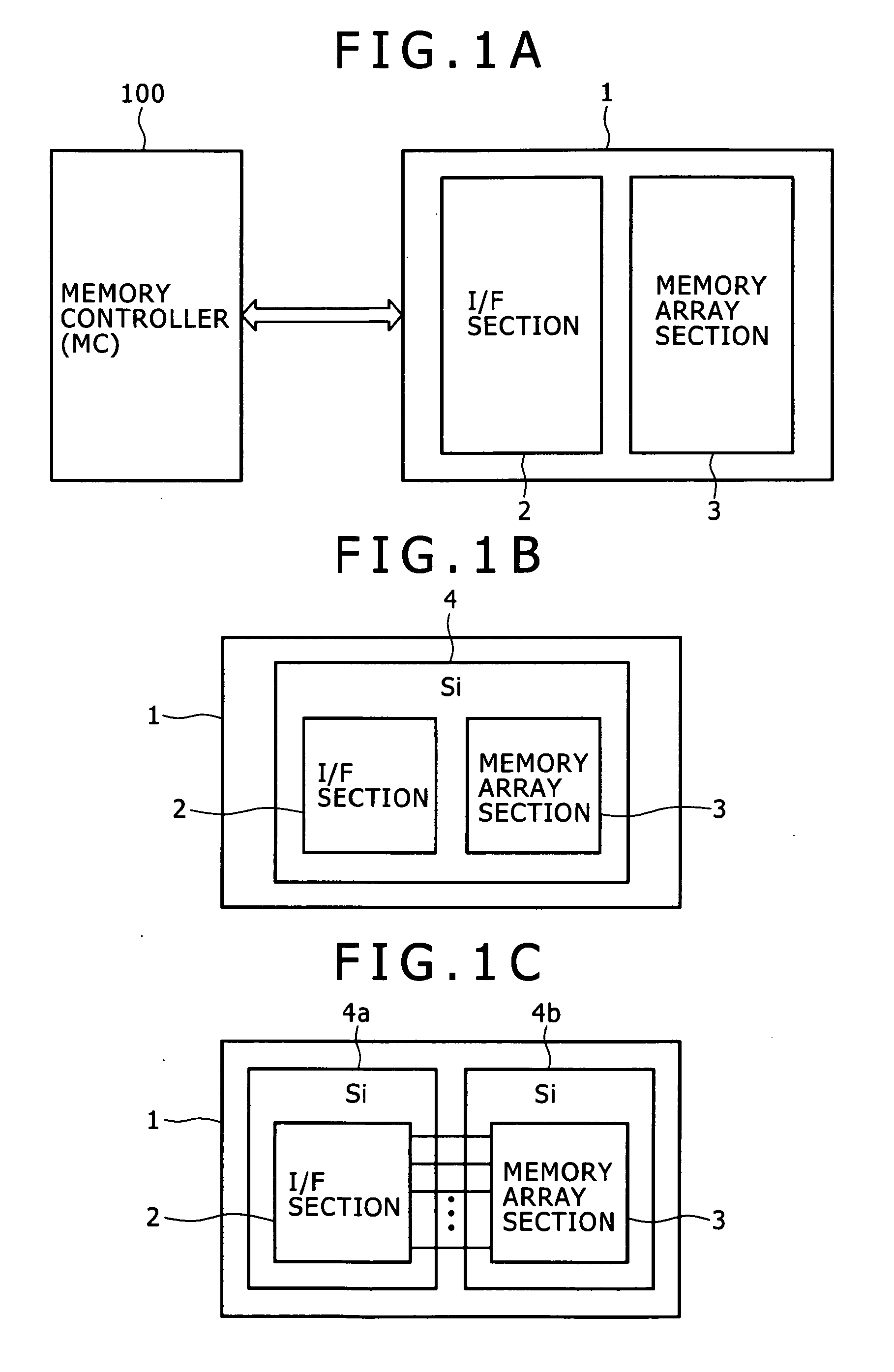
CROSS REFERENCES TO RELATED APPLICATIONS[0001]The present invention contains subject matter related to Japanese Patent Application JP 2008-021710 filed in the Japan Patent Office on Jan. 31, 2008, the entire contents of which being incorporated herein by reference.BACKGROUND OF THE INVENTION[0002]1. Field of the Invention[0003]This invention relates to a semiconductor memory device and an operation method therefor.[0004]2. Description of the Related Art[0005]Various memory types which are different in circuit configuration, operation function and so forth are known for a semiconductor memory device which is used as a RAM (random access memory) chip in various electronic apparatus.[0006]Semiconductor memory devices can be roughly classified into DRAM (Dynamic Random Access Memory) devices and SRAM (Static Random Access Memory) devices from the circuit configuration and the operation.[0007]An SDRAM (Synchronous Dynamic Random Access Memory) is known as a kind of DRAM and outputs data ...
Claims
Application Information
Patent Timeline
Application Date:The date an application was filed.
Publication Date:The date a patent or application was officially published.
First Publication Date:The earliest publication date of a patent with the same application number.
Issue Date:Publication date of the patent grant document.
PCT Entry Date:The Entry date of PCT National Phase.
Estimated Expiry Date:The statutory expiry date of a patent right according to the Patent Law, and it is the longest term of protection that the patent right can achieve without the termination of the patent right due to other reasons(Term extension factor has been taken into account ).
Invalid Date:Actual expiry date is based on effective date or publication date of legal transaction data of invalid patent.

