Microphase-separated structure on flexible substrate, and method of manufacture thereof

Inactive Publication Date: 2009-09-24
FUJIFILM CORP
View PDF1 Cites 59 Cited by
  • Summary
  • Abstract
  • Description
  • Claims
  • Application Information

AI Technical Summary

Benefits of technology

[0006]It is therefore an object of the present invention to provide a structure having a block copolymer layer with a microphase-separated morphology in which a cylindrical or lamellar phase is oriented pe

Problems solved by technology

Moreover, such a process is difficult to carry out over a large surface area and is thus undesirable in terms of productivity.
Finally, in JP 3979470 B, because the block copolymer used is required to have a special structure, this approach lacks general versatility and applicability to other polymers is limited.
Because suff

Method used


Image

  • Microphase-separated structure on flexible substrate, and method of manufacture thereof
  • Microphase-separated structure on flexible substrate, and method of manufacture thereof
  • Microphase-separated structure on flexible substrate, and method of manufacture thereof

Examples


Example

Example 1

[0096]A SiO2 layer (thickness, 50 nm) was formed by vapor-depositing SiO onto a polyimide (PI) film (Upilex-50S; Ube Industries, Ltd.) in an oxygen atmosphere. The surface roughness of the SiO2 layer was 0.91 nm. Following vapor deposition, the film was immediately immersed in a 1.0 wt % toluene solution of octadecyltrimethoxysilane (Gelest, Inc.) and left at rest for one day. The film was then rinsed with toluene and dried, thereby creating a surface-modified polymer substrate 1 on which a layer formed with a silane coupling agent had also been deposited. The layer formed with the silane coupling agent was a monomolecular layer. Assuming the thickness of this layer to be about the chain length of one molecule of the silane coupling agent, from calculations with WinMOPAC (Ver. 3.9.0), the layer thickness was estimated to be about 2.6 nm. Following surface modification, the contact angle with water was 97±6°. The difference between the surface tension of polystyrene (PS) wit...

Example

Example 2

[0098]A SiO2 layer was formed by vapor-depositing SiO onto a polyimide (PI) film (Upilex-50S; Ube Industries, Ltd.) in an oxygen atmosphere. The surface roughness of the SiO2 layer was 0.91 nm. Following vapor deposition, the film was immediately immersed in a 1.0 wt % toluene solution of methoxyphenylpropylmethyldichlorosilane (Gelest, Inc.) and left at rest for one day. The film was then rinsed with toluene and dried, thereby creating a surface-modified polymer substrate 2 on which a layer formed with a silane coupling agent had also been deposited. The layer formed with the silane coupling agent had a thickness, determined by the method described in Example 1 above, of about 1.3 nm. Following surface modification, the contact angle with water was 81±6°. The difference between the surface tension of polystyrene (PS) with the substrate and the surface tension of polymethyl methacrylate (PMMA) with the substrate was 0.1 mN / m.

[0099]A 10.0 wt % toluene solution of PS-b-PMMA (...

Example

Example 3

[0100]A copper layer (thickness, 50 nm) was created by electron beam (EB) vapor-depositing copper onto a polyimide (PI) film (Upilex-50S; Ube Industries, Ltd.) in a vacuum. The film was taken out into the open air, and the surface roughness was measured and found to be 1.08 nm. The film was left to stand out in the open air overnight to allow the surface to oxidize, following which the film was immersed in a 1.0 wt % toluene solution of octadecyltrimethoxysilane (Gelest, Inc.) and left at rest for one day. The film was then rinsed with toluene and dried, thereby creating a surface-modified polymer substrate 3 on which a layer formed with a silane coupling agent had also been deposited. The layer formed with the silane coupling agent had a thickness, determined by the method described in Example 1 above, of about 2.6 nm. Following vapor deposition, the contact angle with water was 21±4°. Following surface modification, the contact angle with water was 107±10°. The difference...


PUM

PropertyMeasurementUnit
Thicknessaaaaaaaaaa
Flexibilityaaaaaaaaaa
Surface roughnessaaaaaaaaaa

Abstract

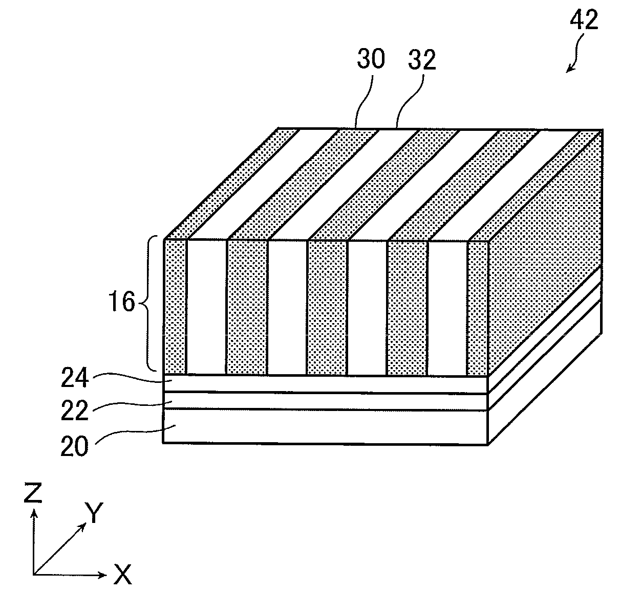
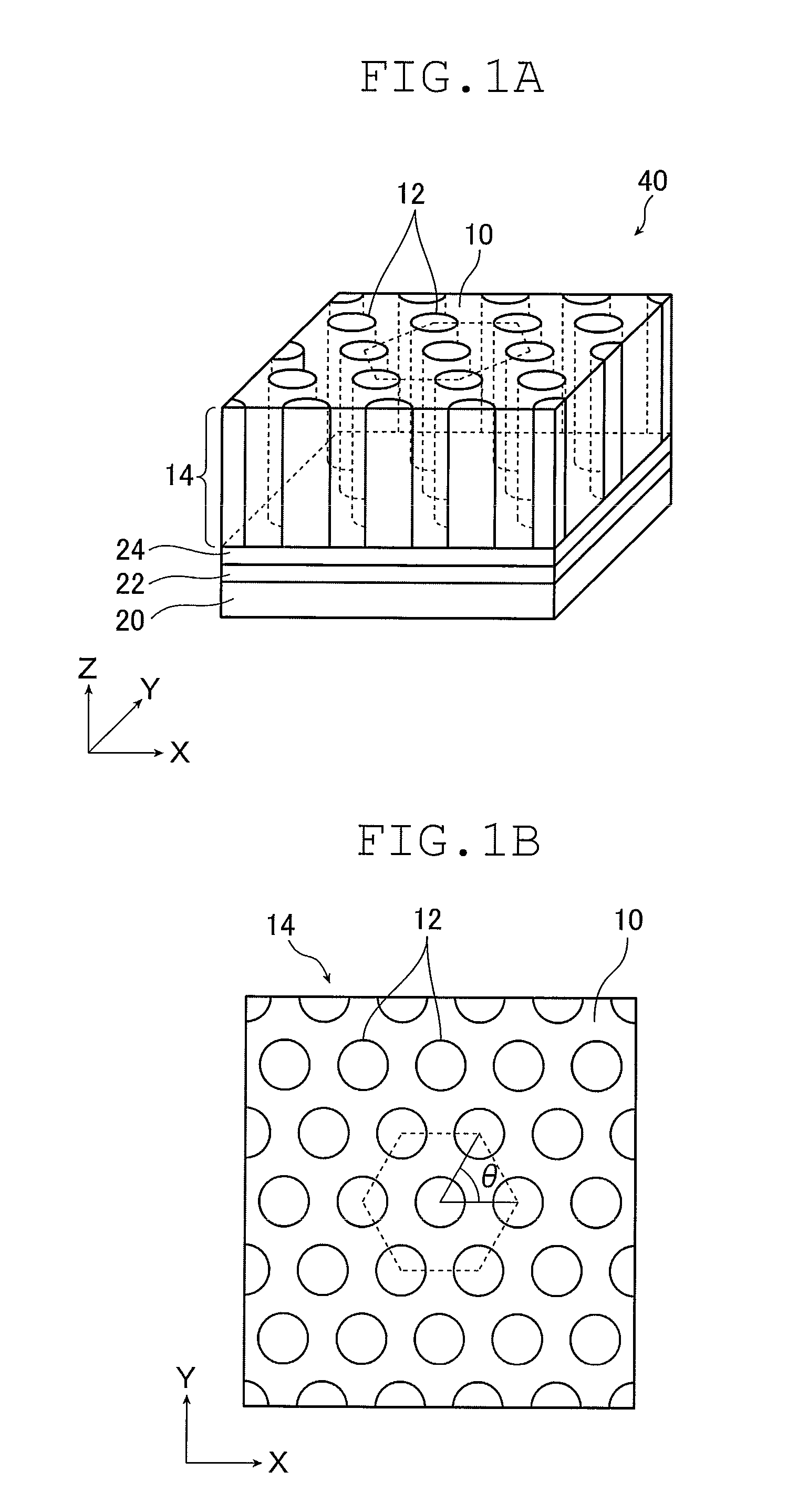
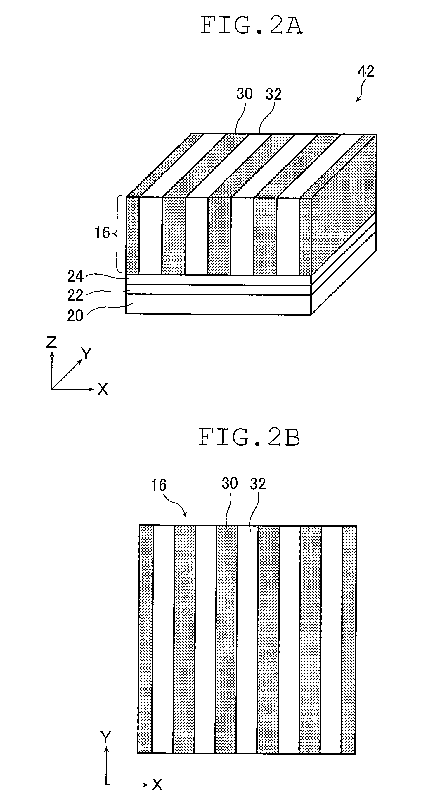
A structure having a block copolymer layer with a microphase-separated morphology in which a cylindrical or lamellar phase is oriented perpendicularly to a flexible substrate such as a polymer substrate is provided. The structure includes a flexible substrate and, in order thereon, a metal oxide layer, a layer formed with a silane coupling agent, and a layer which has a microphase-separated morphology and is formed of a block copolymer obtained by bonding two or more mutually incompatible polymer chains. The microphase-separated morphology has one phase which is lamellar or cylindrical, and oriented perpendicularly to the substrate.

Description

BACKGROUND OF THE INVENTION[0001]The present invention relates to a structure having a metal oxide layer, a layer formed with a silane coupling agent, and a block copolymer layer in this order on a flexible substrate. The invention relates also to a method of manufacturing such a structure.[0002]Recently, in the field of optical materials and electronic materials, there has been a growing demand for greater integration, higher information density, and image information of higher definition. This has led to a need to form a fine, nanometer-scale structure (micropatterning, micropattern structure) in the materials used in this field. In particular, to confer flexibility, handleability and lightweight properties for bendability during use and for lamination onto curved surfaces, there is an acute desire for the high-precision, low-cost manufacture of micropattern structures on flexible substrates such as polymer films.[0003]Micropatterning processes that have been proposed include bott...

Claims


Application Information

Patent Timeline
IPC IPC(8): B32B27/06B05D1/36C08J7/043C08J7/044
CPCB05D1/185B05D3/007B05D3/0254B05D5/00B05D2350/63B82Y30/00C08J2453/00B82Y40/00C08J7/045C08F8/42C08F293/00Y10T428/31663C08J7/0423C08J7/043C08J7/044
Inventor ISHIZUKA, KENICHINISHIMI, TAISEIHORI, RITSUKO
Owner FUJIFILM CORP
Why Eureka
Try Eureka