

Method for fabricating semiconductor structure and structure of static random access memory
a random access memory and semiconductor technology, applied in the direction of semiconductor devices, basic electric elements, electrical appliances, etc., can solve the problems of sudden increase of gate leakage current, increase of direct tunneling possibility, and difficulty in incorporating the high-k dielectric layer into the transistor, so as to avoid the degradation of the layer quality
- Summary
- Abstract
- Description
- Claims
- Application Information
AI Technical Summary
Benefits of technology
Problems solved by technology
Method used
Image

Examples
Embodiment Construction
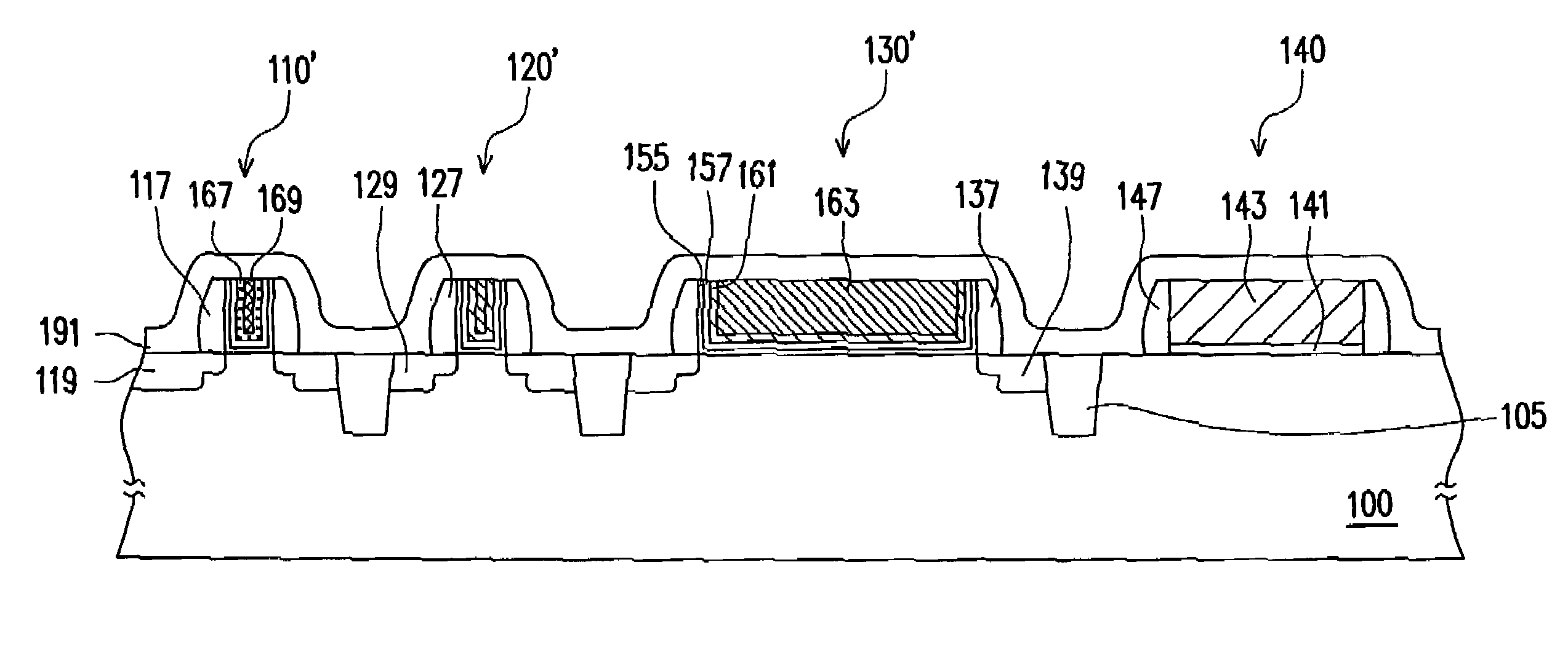
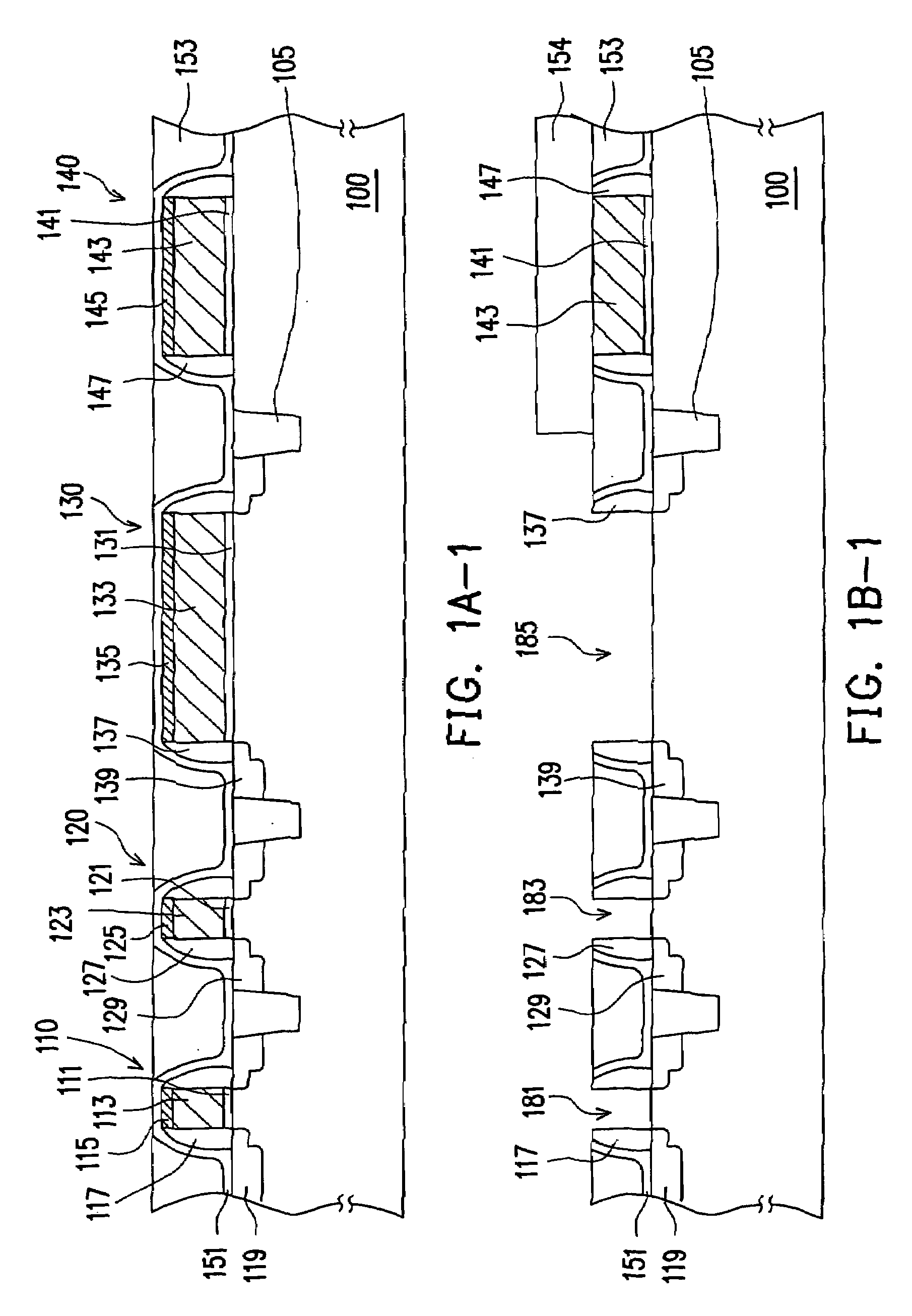
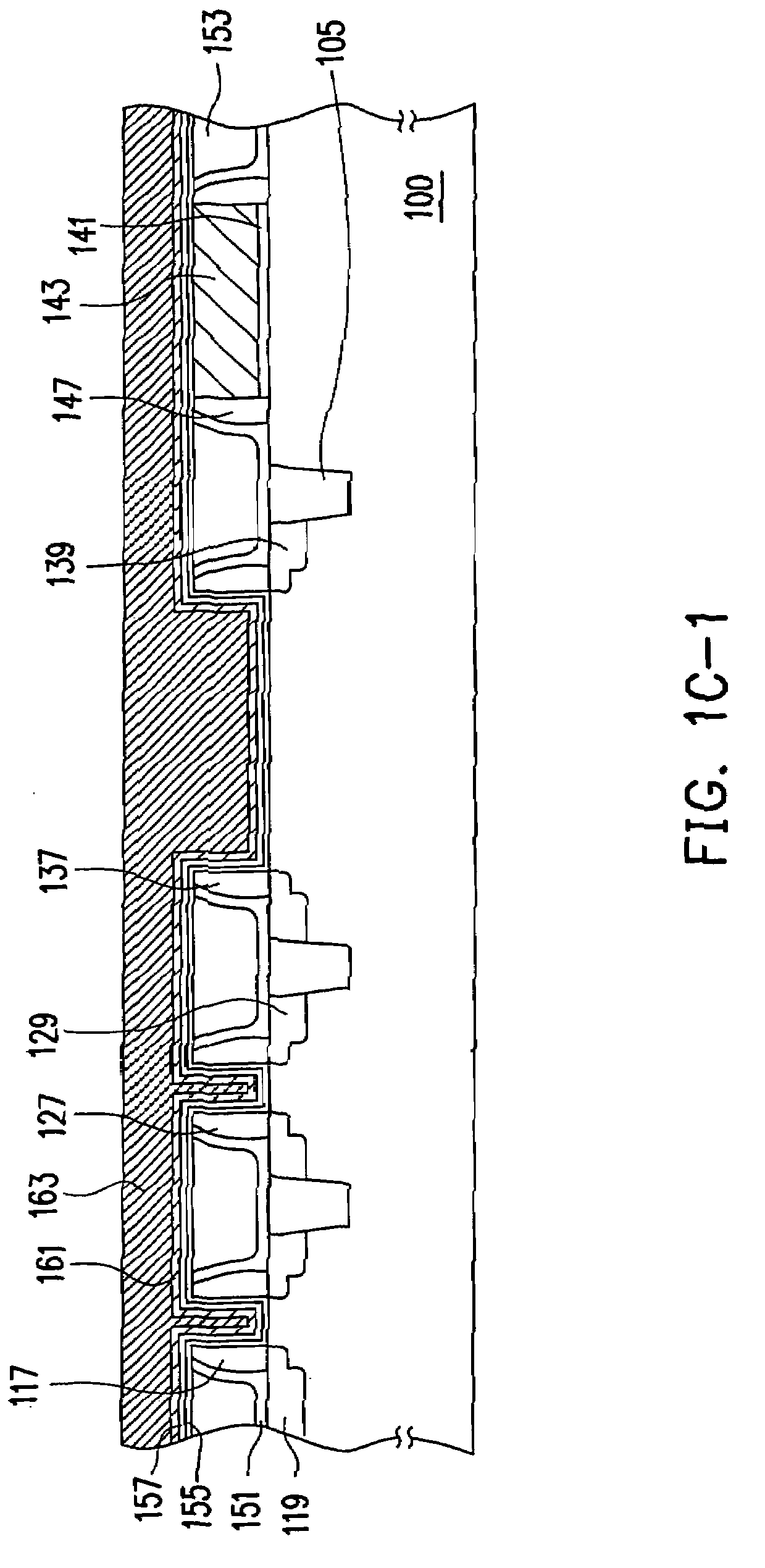
[0034]FIGS. 1A-1 through 1F-1 are cross-sectional views illustrating fabrication process of a semiconductor structure according to one embodiment of the present invention. FIGS. 1A-2 through 1F-2 are cross-sectional views illustrating fabrication process of a static random access memory corresponding to the steps of FIGS. 1A-1 through 1F-1.
[0035]FIG. 1A-1 illustrates a flow chart for fabricating a semiconductor structure according to one embodiment of the present invention. In the illustrated fabrication process, a substrate 100 is first provided. The substrate 100 is, for example, a silicon substrate, a silicon substrate on insulator, a III-V compound semiconductor substrate, or a II-VI compound semiconductor substrate. A first transistor 110, a second transistor 120, a high-voltage element 130 and a resistor 140, which are separated apart by isolation structures 105, have been formed on the substrate 100. The isolation structure 105 is, for example, a shallow trench isolation stru...
PUM
 Abstract
Description
Claims
Application Information