Semiconductor device and manufacturing method of the same

a semiconductor device and manufacturing method technology, applied in the field of semiconductor devices, can solve the problems of poor coupling, reduce the contact area between the wire and the pad, etc., and achieve the effect of improving the electrical properties high pin count of the semiconductor device, and improving the reliability of the semiconductor devi

Active Publication Date: 2009-10-01
RENESAS ELECTRONICS CORP
View PDF1 Cites 49 Cited by
  • Summary
  • Abstract
  • Description
  • Claims
  • Application Information

AI Technical Summary

Benefits of technology

[0023]According to the one aspect of the invention, a rewiring layer can be formed using a conductive film free from pores due to a probe mark. This enables to provide a technology capable of achieving the size reduction, particularly pitch narrowing, of a semiconductor device; a technology capable of achieving a high pin count of a semiconductor device; a technology capable of achieving improvement in the reliability of a semiconductor device; and a technology capable of achieving improvement in electrical properties of a semiconductor device operated at a high speed.

Problems solved by technology

For example, when a wire (which will hereinafter be called “wire” simply) is coupled onto a pad having such a large probe mark, presence of the probe mark reduces a contact area between the wire and the pad, which may lead to a poor coupling problem.

Method used


Image

  • Semiconductor device and manufacturing method of the same
  • Semiconductor device and manufacturing method of the same
  • Semiconductor device and manufacturing method of the same

Examples


embodiment 1

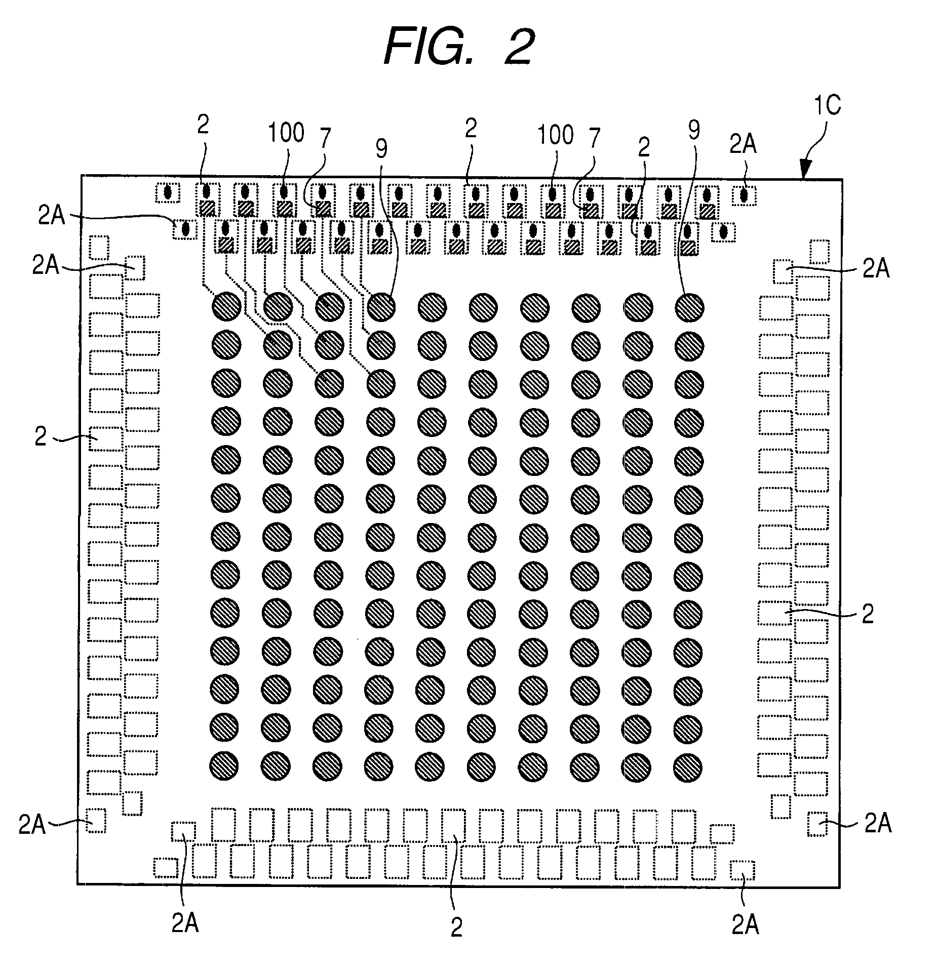
[0066]First, the configuration of a semiconductor device according to this embodiment will be described referring to some drawings. FIG. 2 is a schematic plan view of the semiconductor device according to this embodiment; FIG. 3 is a fragmentary cross-sectional schematic view of the semiconductor device illustrated in FIG. 2; and FIG. 4 is a fragmentary schematic plan view of the semiconductor device shown in FIG. 2. FIG. 4 however illustrates the device after removal of a portion thereof.

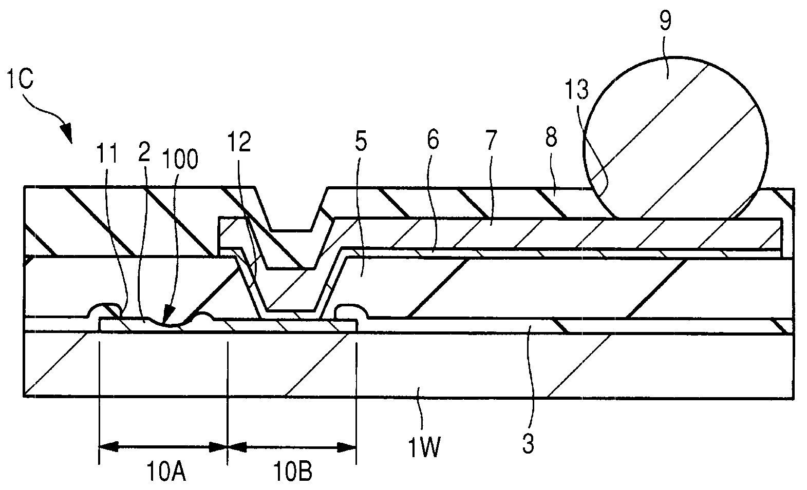
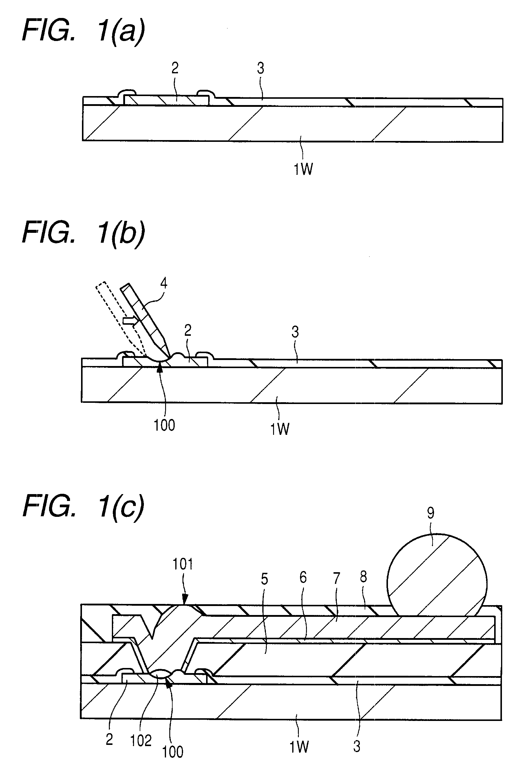
[0067]The semiconductor device according to this embodiment is comprised of a semiconductor chip 1C having a BGA (Ball Grid Array) structure. The semiconductor chip 1C has, at the center portion thereof, bump electrodes 9 in the ball form arranged into a matrix. The bump electrodes 9 are each placed as an external electrode of the semiconductor chip 1C so as to protrude from a passivation film 8 which will be a surface protective film. In FIG. 2, pads (electrodes) 2 placed at the periphery of the s...

embodiment 2

[0103]In the above embodiment, the rewiring layer is comprised of a conductive film (plating film) formed by plating. In this embodiment, on the other hand, a bump electrode is made of a plating film. Embodiment 2 is similar to Embodiment 1 except for the above-described difference.

[0104]The configuration of the semiconductor device according to this embodiment will be described first referring to some drawings. FIG. 14 is a schematic plan view of the semiconductor device according to this embodiment; FIG. 15 is a fragmentary cross-sectional schematic view of the semiconductor device illustrated in FIG. 14; and FIG. 16 is a fragmentary schematic plan view of the semiconductor device illustrated in FIG. 14.

[0105]A rectangular semiconductor chip 1C configuring the semiconductor device of this embodiment has, on the main surface thereof, a semiconductor circuit (for example, LSI) not illustrated. A pad 2 electrically coupled to an interconnect configuring the semiconductor circuit and ...

embodiment 3

[0124]In Embodiment 1, the bump electrode is formed on a portion of the rewiring layer by using solder printing technology. In the present embodiment, on the other hand, a pad is formed on a portion of a rewiring layer by using plating. Embodiment 3 is similar to Embodiment 1 except for the above-described difference.

[0125]FIGS. 23 and 24 are each a fragmentary cross-sectional schematic view of a semiconductor device during manufacturing steps thereof according to this embodiment. The step described referring to FIG. 23 follows the step described in Embodiment 1 referring to FIG. 11 so that steps subsequent thereto will hereinafter be described.

[0126]As illustrated in FIG. 23, a resist film formed by the method of application over the semiconductor wafer 1W is patterned by photolithography to form a mask 24 having an opening portion 25 from which a portion of a rewiring layer 7 comprised of, for example, a Cu / Ni film is exposed. Then, a pad 26 made of a conductive film (plating film...


PUM


Abstract

Provided is a semiconductor device having a pad on a semiconductor chip, a first passivation film formed over the semiconductor chip and having an opening portion on the pad of a probe region and a coupling region, a second passivation film formed over the pad and the first passivation film and having an opening portion on the pad of the coupling region, and a rewiring layer formed over the coupling region and the second passivation film and electrically coupled to the pad. The pad of the probe region placed on the periphery side of the semiconductor chip relative to the coupling region has a probe mark and the rewiring layer extends from the coupling region to the center side of the semiconductor chip. The present invention provides a technology capable of achieving size reduction, particularly pitch narrowing, of a semiconductor device.

Description

CROSS-REFERENCE TO RELATED APPLICATIONS[0001]The disclosure of Japanese Patent Application No. 2008-92633 filed on Mar. 31, 2008 including the specification, drawings and abstract is incorporated herein by reference in its entirety.BACKGROUND OF THE INVENTION[0002]The present invention relates to a semiconductor device and a manufacturing technology thereof. In particular, the invention pertains to a technology effective when applied to the manufacture of a semiconductor device having a conductive film formed, after a probe test step is performed by bringing a probe needle into contact with a pad, on the pad by plating.[0003]In a probe test step (test step) of a semiconductor device equipped with a semiconductor circuit (for example, LSI), electrical properties are measured by bringing a probe needle (probe) into contact with the surface of a pad formed over a semiconductor wafer. Since this probe needle is made of a hard metal such as W (tungsten) and has a sharp top, it inevitably...

Claims


Application Information

Patent Timeline
Patent Type & Authority Applications(United States)
IPC IPC(8): H01L23/48H01L21/66
CPCH01L22/14H01L22/20H01L22/32H01L24/05H01L24/06H01L24/11H01L24/12H01L24/48H01L24/49H01L25/0657H01L2224/02313H01L2224/04042H01L2224/05073H01L2224/05082H01L2224/05187H01L2224/05552H01L2224/05624H01L2224/05644H01L2224/1132H01L2224/13099H01L2224/13144H01L2224/16225H01L2224/32145H01L2224/45124H01L2224/45144H01L2224/48091H01L2224/4813H01L2224/48145H01L2224/48227H01L2224/48465H01L2224/4847H01L2224/4911H01L2224/49429H01L2224/49431H01L2224/85951H01L2225/0651H01L2225/06517H01L2924/01002H01L2924/01004H01L2924/01005H01L2924/01013H01L2924/01014H01L2924/01015H01L2924/01022H01L2924/01028H01L2924/01029H01L2924/01046H01L2924/01047H01L2924/0105H01L2924/01074H01L2924/01078H01L2924/01079H01L2924/01082H01L2924/01083H01L2924/014H01L2924/05042H01L2924/10329H01L2924/15311H01L2924/19041H01L2924/19043H01L2924/30105H01L2924/01006H01L2924/01019H01L2924/01033H01L2224/32225H01L2224/73204H01L2224/73265H01L2224/48624H01L2224/48644H01L2224/48724H01L2224/0401H01L2224/05012H01L2224/05553H01L2224/05554H01L2224/05555H01L2924/12041H01L2224/02166H01L2224/0603H01L2224/11334H01L2224/10G01R31/26H01L2924/1306H01L2924/00014H01L2924/04941H01L2924/04953H01L2924/00H01L2224/48744H01L2924/00012H01L2924/181H01L24/45H01L24/73H01L2224/0392H01L2224/0235H01L22/30H01L24/13H01L2224/02371H01L24/03H01L2224/02373H01L2224/02381H01L2224/05558H01L2224/06133H01L2224/06135H05K999/99
Inventor AKIBA, TOSHIHIKOYASUMURA, BUNJISATO, MASANAOABE, HIROMI
Owner RENESAS ELECTRONICS CORP
Why Eureka
Try Eureka