Single Event Upset error detection within sequential storage circuitry of an integrated circuit

a technology of integrated circuits and error detection circuits, applied in the direction of transmission, instruments, electric digital data processing, etc., can solve the problems of inability to apply sequential storage circuits, inability to detect and correct errors in multiple bits, and prohibitive computational and storage overhead, so as to reduce the likelihood of error detection circuits, reduce the likelihood of errors, and be more robust to soft errors

Active Publication Date: 2009-10-01
ARM LTD
View PDF99 Cites 34 Cited by
  • Summary
  • Abstract
  • Description
  • Claims
  • Application Information

AI Technical Summary

Benefits of technology

[0026]If a neutron or alpha particle strike hits the additional storage element, then the error detection circuitry will still detect an error, and in this case an error will be flagged even when there is no real state corruption (the system as a whole is only concerned with the data stored in the first and second storage elements and does not make use of the data stored in the additional storage element). In one embodiment, to reduce the instances of such false error detection situations, the additional storage element may be designed to be robust to single event upset errors, thereby reducing the likelihood of the error detection circuitry detecting a difference in the input data value due to a single event upset error occurring in the additional storage element. Since this additional storage element is not on the critical path, various known techniques can be used to make it mo

Problems solved by technology

Errors can occur due to SEU if it leads to a state flip in the state-holding elements that determine the architectural state of the integrated circuit, such as the RAM arrays, the Register File, the architectural-state registers of a processor, or the flip-flops and latches within control logic.
However, the ability to detect and correct errors in multiple bits requires fairly sophisticated ECC algorithms with prohibitive computational and storage overhead.
However, the same technique cannot be applied to sequential storage circuitry such as latches and flip-flops, due to their spatial distribution throughout the integrated circuit, and due to the fact that neutron and particle strikes in such distributed logic (as opposed to RAM memory) can cause separate bit failures within multiple of the sequential storage circuits, which ECC cannot correct.
These known techniques hence disadvantageously increase the amount of circuit area needed and the power consumed.
Timing errors occur in a Razor-like system when propagation de

Method used


Image

  • Single Event Upset error detection within sequential storage circuitry of an integrated circuit
  • Single Event Upset error detection within sequential storage circuitry of an integrated circuit
  • Single Event Upset error detection within sequential storage circuitry of an integrated circuit

Examples


Embodiment Construction

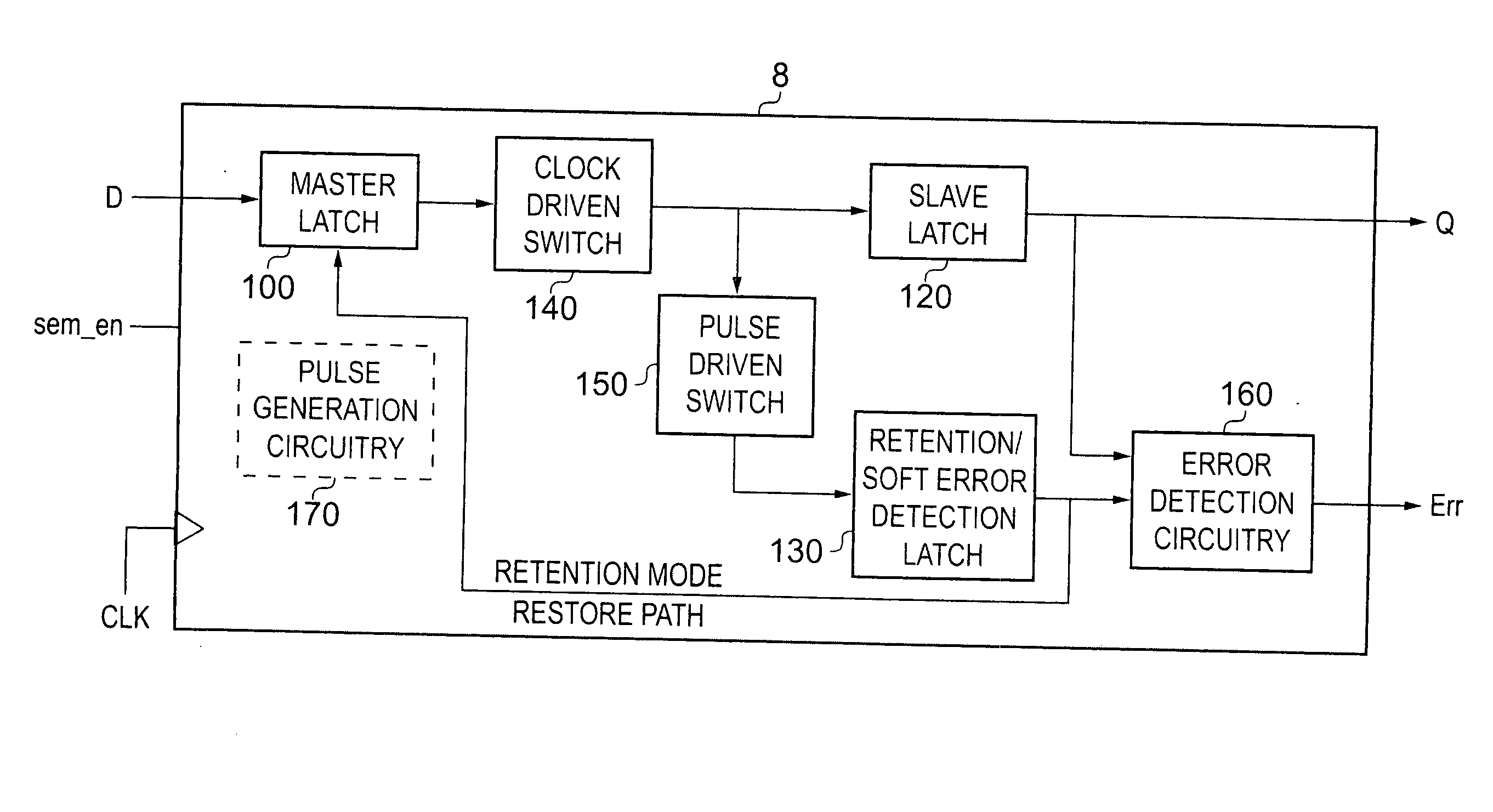
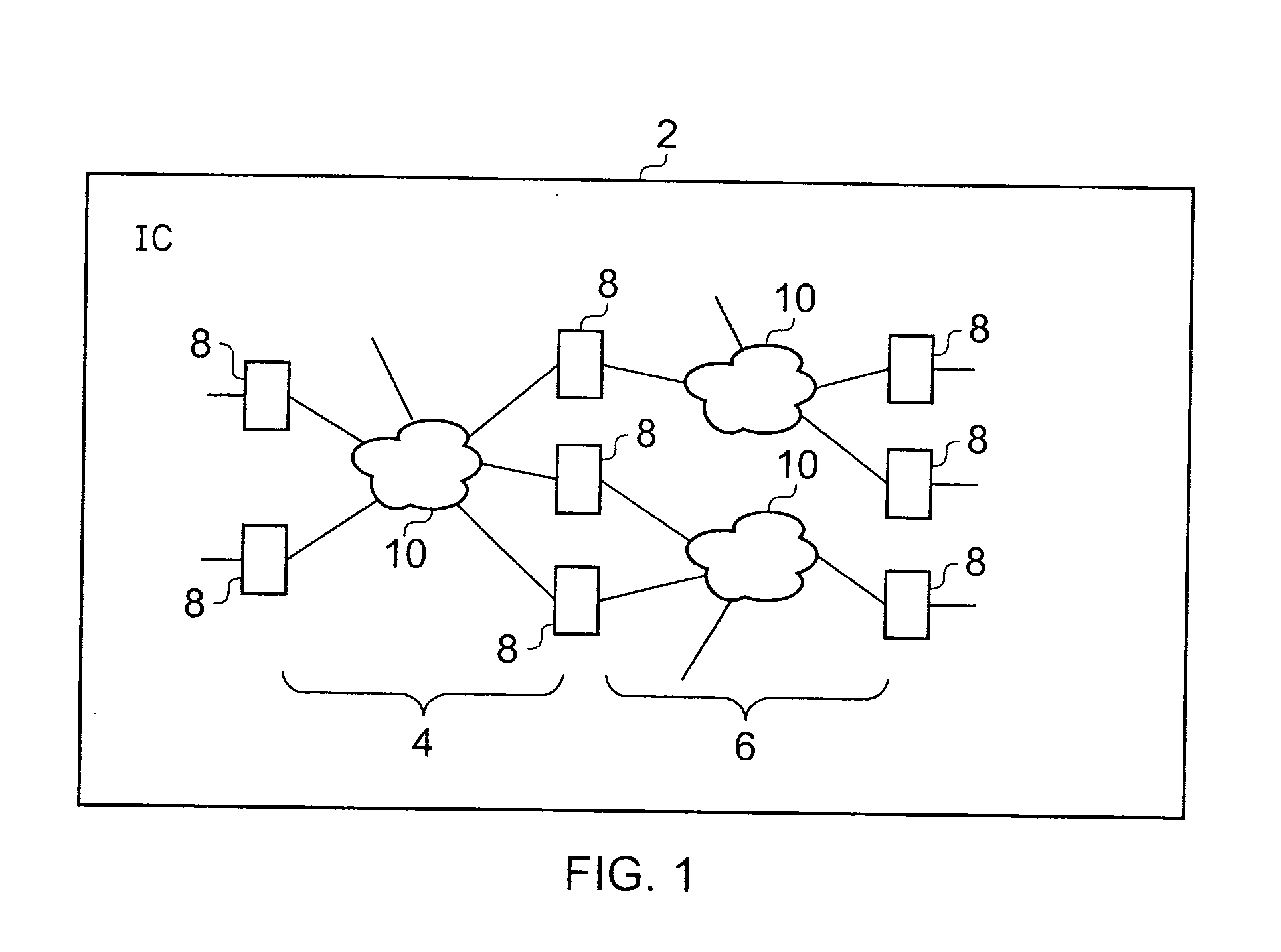
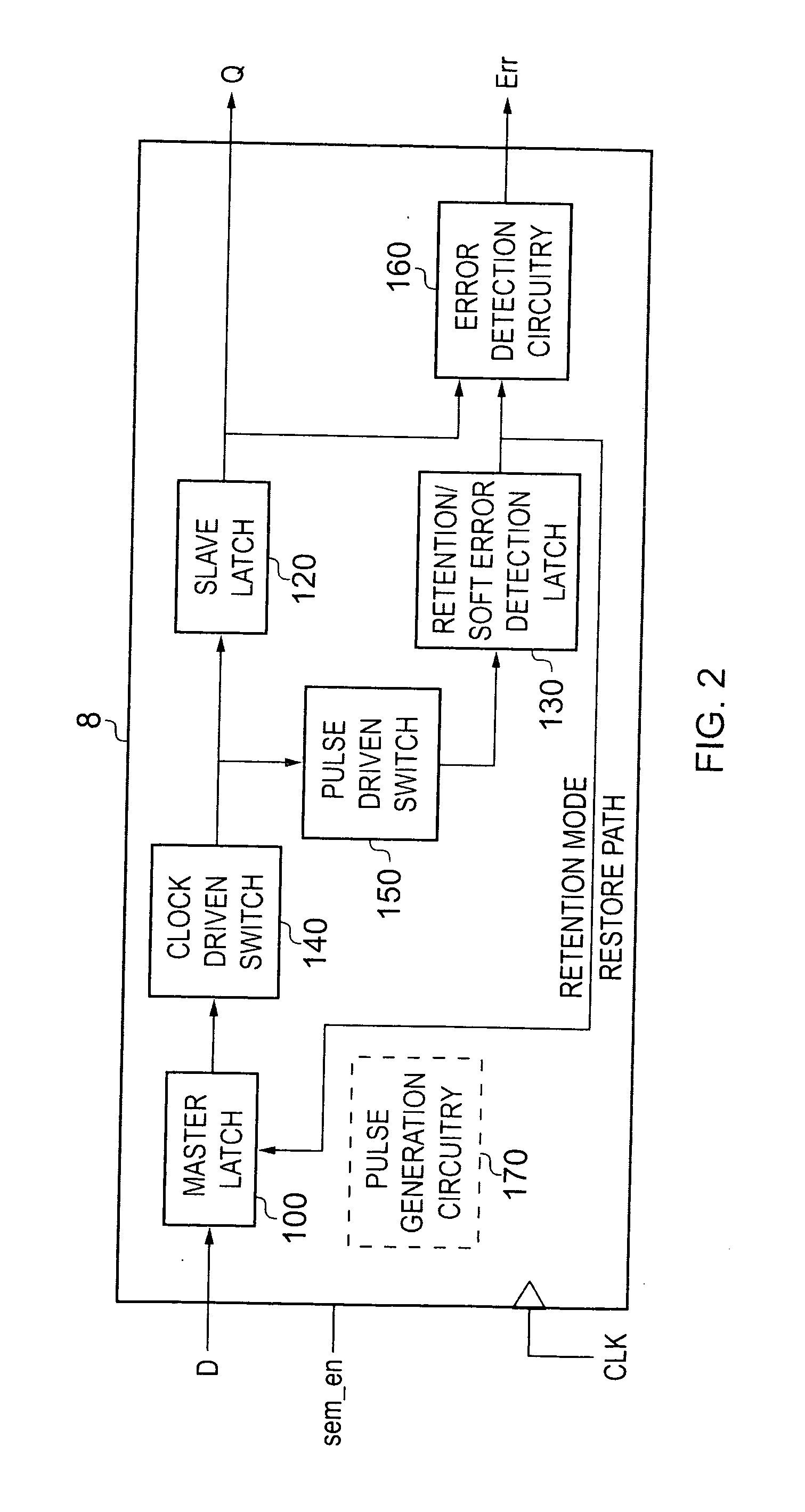
[0043]FIG. 1 shows an integrated circuit 2 including pipeline stages 4, 6 extending between sequential edge-triggered storage circuits 8 which may be in the form of flip-flops. Between the sequential storage circuits 8 are respective instances of combinatorial logic circuitry 10, which serve to receive signals from one or more preceding stages and generate signals to be passed to one or more succeeding stages. The period of time between the capture of signal values by the sequential storage circuits 8 for successive clock periods is the time that is available for the combinatorial logic circuitry 10 to evaluate its inputs so as to generate its outputs. Embodiments of the present invention provide a new design for the sequential storage circuit 8, which can detect SEUs occurring within the sequential storage circuit due to neutron or alpha particle strikes on the sequential storage circuit.

[0044]FIG. 2 is a block diagram schematically illustrating a sequential storage circuit in acco...


PUM


Abstract

Sequential storage circuitry for a integrated circuit is provided, comprising a first storage element, a second storage element and an additional storage element. The first storage element stores, during a first phase of a clock signal, a first indication of an input data value received by the sequential storage circuitry. The second storage element is coupled to an output of the first storage element, and stores a second indication of the input data value during a second phase of the clock signal. The additional storage element is driven by a pulse signal derived from the clock signal, and is arranged on occurrence of that pulse signal to store a third indication of the input data value. Error detection circuitry is then provided for detecting a single event upset error in either the first storage element or the second storage element. In particular, during the first phase of the clock signal, the error detection circuitry detects the single event upset error in the first storage element if there is a difference in the input data value as indicated by the first indication and the third indication. Further, during the second phase of the clock signal, the error detection circuitry detects a single event upset error in the second storage element if there is a difference in the input data value as indicated by the second indication and the third indication. Such an arrangement provides a simple mechanism for detecting soft errors in both the first storage element and the second storage element using only one additional storage element.

Description

BACKGROUND OF THE INVENTION[0001]1. Field of the Invention[0002]This invention relates to the detection of single event upset errors within sequential storage circuitry of integrated circuits, such as those which arise from neutron and alpha particle strikes.[0003]2. Description of the Prior Art[0004]A Single Event Upset (SEU) (also known as a soft error) is a change in state or a transient voltage pulse at sensitive nodes in integrated circuits, such as processors. SEUs occur due to high energy neutron or alpha particle strikes on the silicon substrate of processors. Errors can occur due to SEU if it leads to a state flip in the state-holding elements that determine the architectural state of the integrated circuit, such as the RAM arrays, the Register File, the architectural-state registers of a processor, or the flip-flops and latches within control logic. In the context of this document, we consider an error due to SEU as a state flip in any state-holding element inside the inte...

Claims


Application Information

Patent Timeline
IPC IPC(8): H04L1/00G06F11/07
CPCG06F11/00
Inventor CHANDRA, VIKASIDGUNJI, SACHIN SATISH
Owner ARM LTD
Why Eureka
Try Eureka