Method for manufacturing organic transistor and organic transistor

a manufacturing method and organic semiconductor technology, applied in the direction of thermoelectric device junction materials, electrical apparatus, semiconductor devices, etc., can solve the problems of poor product quality, complicated process, high cost, etc., and achieve the effects of improving the crystal properties of organic semiconductor materials, easy removal, and high reliability

Inactive Publication Date: 2009-10-15
DAI NIPPON PRINTING CO LTD +1
View PDF4 Cites 19 Cited by
  • Summary
  • Abstract
  • Description
  • Claims
  • Application Information

AI Technical Summary

Benefits of technology

[0016]In the present invention, the hydrophobic substrate preferably comprises: a hydrophilic substrate exhibiting hydrophilicity on a surface thereof, and a hydrophobic layer formed on the hydrophilic substrate and made of a self-assembled monolayer exhibiting hydrophobicity, and the step of forming a hydrophobic/hydrophilic pattern substrate is preferably a step of removing the hydrophobic layer in pattern and exposing the hydrophilic substrate surface in pattern. As the hydrophobic layer made of a self-assembled monolayer can be easily removed by means such as an ultraviolet irradiation, production of a hydrophobic/hydrophilic pattern substrate having a highly-precise hydrophobic/hydrophilic pattern in the step of forming a hydrophobic/hydrophilic pattern substrate can be made possible.
[0017]Further, in the present invention, the insulating functional material preferably has a function of improving crystal properties of the organic semiconductor material contained in the organic semiconductor layer. As the insulating functional material has such function, the organic transistor produced by the present invention can be a highly-reliable organic transistor even when the transistor is either of a top gate type structure or a bottom gate type structure. As the insulating functional material has such function, the organic transistor produced by the present invention can be a highly-reliable organic transistor even when the transistor is either of a top gate type structure or a bottom gate type structure.
[0018]The present invention further provides an organic transistor comprising: a hydrophobic/hydrophilic pattern substrate having a hydrophobic region and a hydrophilic region formed in pattern on a surface thereof, a lyophilic functional layer, made of an insulating functional material and having higher lyophilic properties to an organic solvent than that of the hydrophobic region, formed on the hydrophilic region, and an

Problems solved by technology

However, the vacuum deposition method has a problem of being poor in its productivity because vacuum conditions need to be fulfilled, a large amount of organic semiconductor materials adhered to a mask

Method used


Image

  • Method for manufacturing organic transistor and organic transistor
  • Method for manufacturing organic transistor and organic transistor
  • Method for manufacturing organic transistor and organic transistor

Examples


first embodiment

Hydrophobic Substrate of First Embodiment

[0047]First, a hydrophobic substrate of the first embodiment will be explained. The hydrophobic substrate of the present embodiment is not particularly limited as long as the substrate is made of a hydrophobic material which can be provided with hydrophilicity by conducting the predetermined hydrophilic treatment. Such hydrophobic material may be an organic material or an inorganic material. As the hydrophobic material used for the hydrophobic. substrate of the present embodiment, materials such as polyimide, polyester, polyethylene, polyphenylene sulfide, polyparaxylene, polyethylene terephthalate, polyethylene naphthalate, and polydimethylsiloxane can be cited. Any of these hydrophobic materials can be used in the present embodiment. Further, only a hydrophobic material of a single kind, or alternatively, hydrophobic materials of plural kinds may be used.

[0048]As a thickness of the hydrophobic substrate of the present embodiment, it is not ...

second embodiment

Hydrophobic Substrate of Second Embodiment

[0049]Next, a hydrophobic substrate of the second embodiment will be explained. The hydrophobic substrate of the present embodiment is a substrate comprising a hydrophilic substrate which exhibits hydrophilicity on its surface and a hydrophobic layer formed on the hydrophilic substrate which exhibits hydrophobicity on its surface.

Hydrophilic Substrate

[0050]The hydrophilic substrate used in the present embodiment is not particularly limited as long as the surface thereof exhibits the desired hydrophilicity. Here, “hydrophilicity” means a state where a contact angle to water at 25° C. is 40 ° or smaller. The hydrophilicity which the hydrophilic substrate used in the present step is preferably a state where a contact angle to water at 25° C. is 40° or smaller, more preferably 30° or smaller, and even more preferably 20° or smaller.

[0051]A material constituting the hydrophilic substrate used for the present embodiment (hereinafter, “hydrophilic ...

example 1

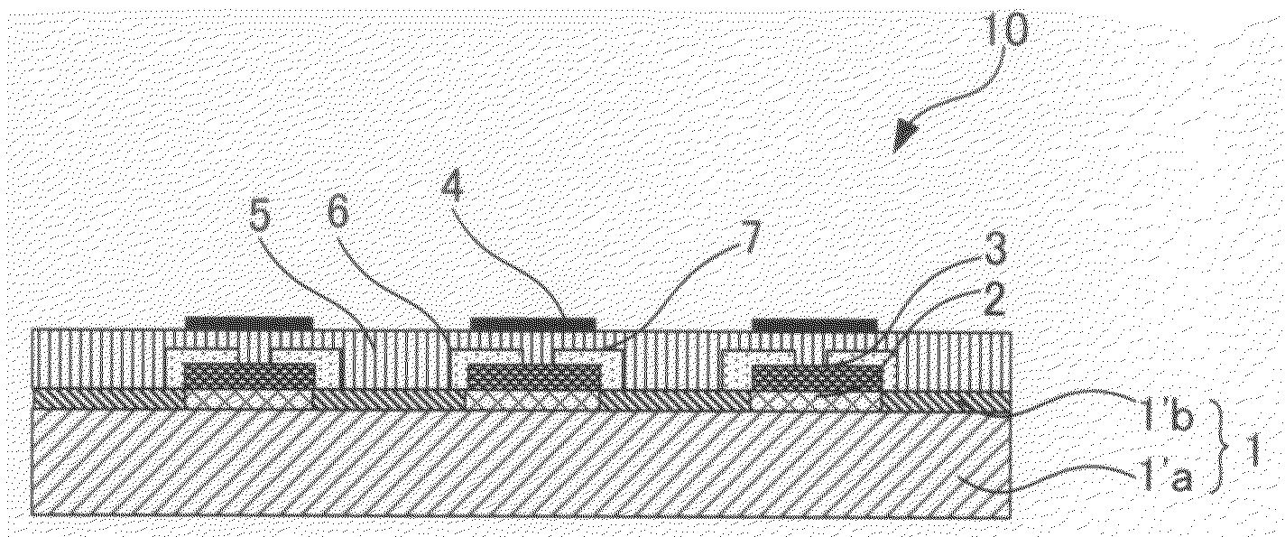
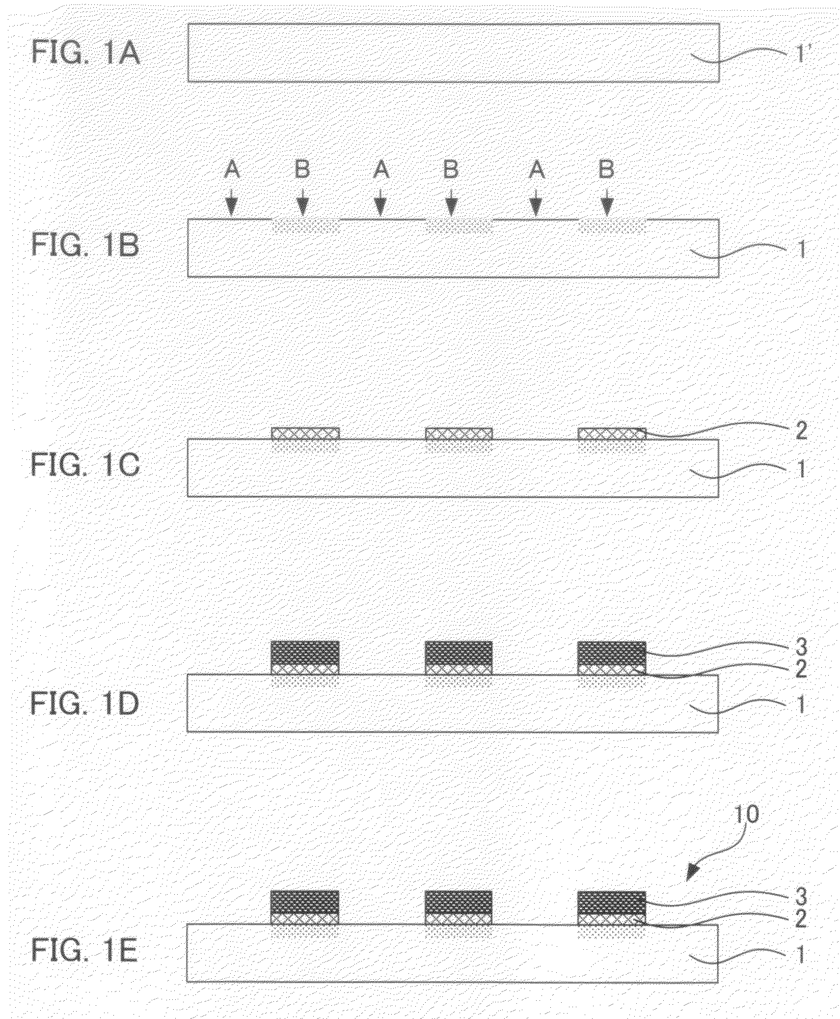
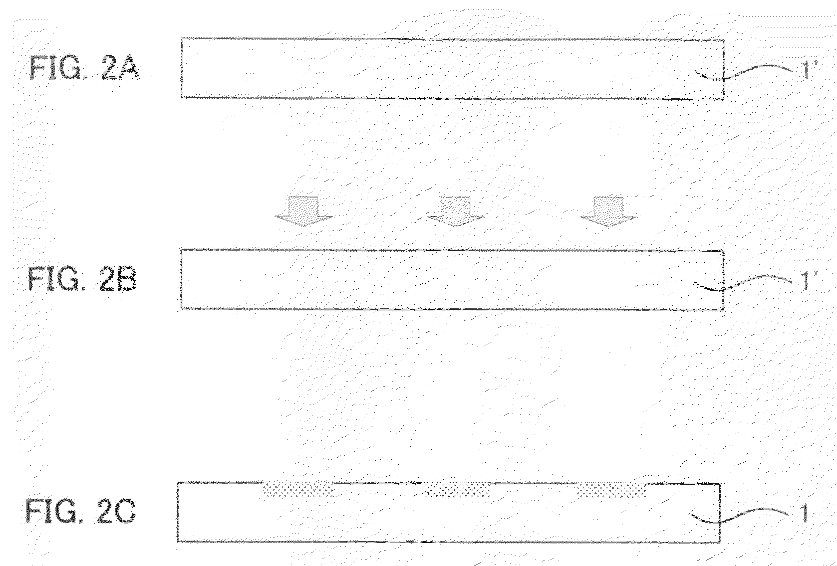
[0124]An HMDS (hexamethyldisilazane) was formed on a silicon wafer with a thermally-oxidized film (50 nm) attached thereto and a hydrophobic layer is produced. Ultraviolet of wavelength of 185 nm was radiated through a metal mask having an opening for three minutes by using a device manufactured by SEN LIGHTS CORPORATION. By decomposing the HMDS in the opening, a hydrophilic region was obtained. The substrate was dipped into a chloroform fluid of PhTS (β-phenethyltrichlorosilane) and a PhTS monolayer was formed in the hydrophilic region as an insulating functional material. A toluene fluid of octyl quarter thiophene (8QT8) (0.3 wt %) was then coated on the substrate to evaporate the solvent, and an 8QT8 thin film was formed only in the hydrophilic region. Using a vacuum deposition device manufactured BY ULVAC, INC., a deposited film of Au was formed by 30 nm and an organic transistor (device 1) was produced.


PUM


Abstract

A method of producing an organic transistor which can form directly an organic semiconductor layer in pattern by simple processes and can produce an organic transistor excellent in transistor characteristics. The method includes: forming a hydrophobic/hydrophilic pattern substrate, in which a hydrophobic/hydrophilic pattern substrate is formed by using a hydrophobic substrate and by forming the hydrophilic region in pattern on the hydrophobic surface; forming a lyophilic functional layer, in which a lyophilic functional layer, made of an insulating functional material having the predetermined characteristics and having higher lyophilic properties to an organic solvent than that of the hydrophobic region, is formed on the hydrophilic region; forming an organic semiconductor layer, in which an organic semiconductor layer is formed on the lyophilic functional layer by selectively coating a coating solution for forming an organic semiconductor layer, which has an organic semiconductor material and an organic solvent, to the lyophilic functional layer.

Description

BACKGROUND OF THE INVENTION[0001]1. Field of the Invention[0002]The present invention relates to a method of producing an organic transistor which enables a simultaneous production of plural organic transistors, and an organic transistor which can be produced by the above-mentioned method of producing an organic transistor.[0003]2. Description of the Related Art[0004]A semiconductor transistor typified by TFT shows the current trend towards spreading of its applications along with the development of display devices. Such a semiconductor transistor functions as a switching element when the electrodes are connected through a semiconductor material.[0005]As the semiconductor material used for the semiconductor transistor, inorganic semiconductor materials such as silicon (Si), gallium arsenic (GaAs) and indium gallium arsenic (InGaAs) have been used. Semiconductor transistors using such an inorganic semiconductor material are also used for display TFT array substrates of liquid crystal...

Claims


Application Information

Patent Timeline
IPC IPC(8): H01L51/30H01L51/40
CPCH01L27/283H01L51/0545H01L51/0012H10K19/10H10K71/191H10K10/466
Inventor KANO, MASATAKATSUKAGOSHI, KAZUHITOMINARI, TAKEO
Owner DAI NIPPON PRINTING CO LTD
Why Eureka
Try Eureka