Multi-layer circuit substrate and motor drive circuit substrate
- Summary
- Abstract
- Description
- Claims
- Application Information
AI Technical Summary
Benefits of technology
Problems solved by technology
Method used
Image

Examples
modified example
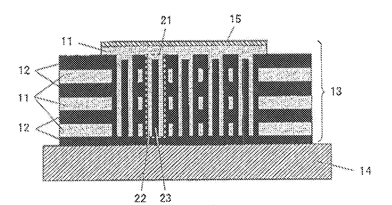
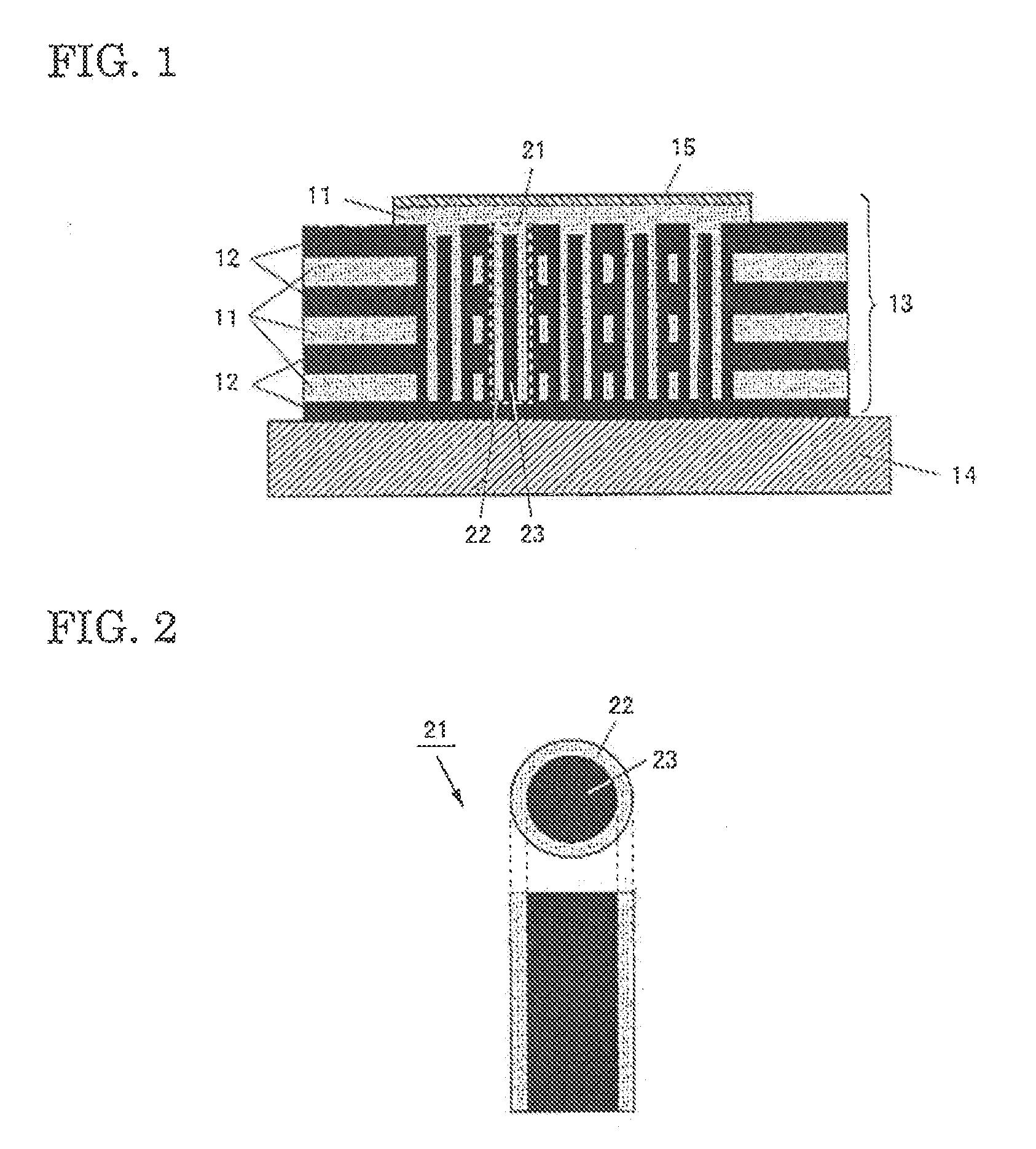
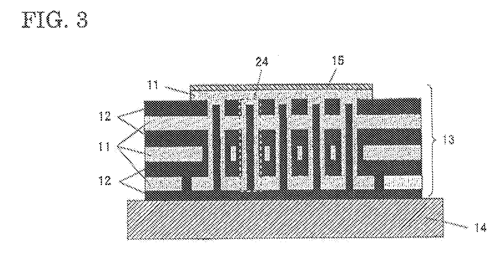
[0064]In the present embodiment, a description was given for a case where the conducting layers 11 are made of copper. In place of copper, the conducting layers may be made of metals such as aluminum, nickel, silver, titanium and gold, their alloys the surface of which is laminated by plating with nickel or nickel / gold. Further, these metals, alloys and laminated films may be formed by pressure bonding, sputtering, chemical vapor deposition, vacuum deposition, thick film printing or a combination of these methods. The thick film printing is preferable, with consideration given to the fact that the conducting layers 11 are approximately 100□m in thickness.
[0065]In the present embodiment, a description was given for a case where all insulating layers 12 inside the laminated circuit portion 13 are made of a prepreg. It is acceptable that only an insulating layer 12, which is the lowermost layer, is made of a diamond like carbon layer (DLC layer). In this case, the DLC layer is made up ...
PUM
 Abstract
Description
Claims
Application Information
 - Generate Ideas
- Intellectual Property
- Life Sciences
- Materials
- Tech Scout
- Unparalleled Data Quality
- Higher Quality Content
- 60% Fewer Hallucinations
Browse by: Latest US Patents, China's latest patents, Technical Efficacy Thesaurus, Application Domain, Technology Topic, Popular Technical Reports.
© 2025 PatSnap. All rights reserved.Legal|Privacy policy|Modern Slavery Act Transparency Statement|Sitemap|About US| Contact US: help@patsnap.com