Electronic device

a technology of infrared sensor and thermal infrared image sensor, which is applied in the field of electronic devices, can solve the problems of not easy to reduce the size or manufacturing cost of such a quantum sensor, difficult to apply it to cars, crime prevention tools, etc., and achieves the effect of reducing noise, reducing the escape of heat from the heat storage portion to the outside, and improving heat insulation properties

Active Publication Date: 2009-10-22
PANASONIC CORP
View PDF13 Cites 11 Cited by
  • Summary
  • Abstract
  • Description
  • Claims
  • Application Information

AI Technical Summary

Benefits of technology

[0046]In the electronic device of the present invention, heat continues to be stored mostly in the infrared ray absorbing section with the heat sensing section and the infrared ray absorbing section spatially separated from each other except during reading. That is why the escape of the heat from the heat storage portion to the outside can be minimized. Besides, since the interconnect that connects together the heat sensing section and the detector circuit section can be kept connected, no noise will be produced by repeatedly turning the interconnect from in-contact state into out-of-contact state, or vice versa. Thus, according to the present invention, the heat insulation property can be improved between the heat storage section and the outside, and therefore, the temperature changes significantly depending on the quantity of the incident infrared radiation. In addition, since the noise produced by the contact resistance is just a negligible level, the infrared ray can be detected with SNR and accuracy both increased.

Problems solved by technology

That is why it is difficult to reduce the size or manufacturing cost of such a quantum sensor and it is not easy to apply it to cars, crime prevention tools and various other consumer electronic products.
On the other hand, a thermal sensor has lower sensitivity than a quantum sensor but needs no cooling mechanism to maintain low temperatures.

Method used


Image

  • Electronic device
  • Electronic device
  • Electronic device

Examples


embodiment 1

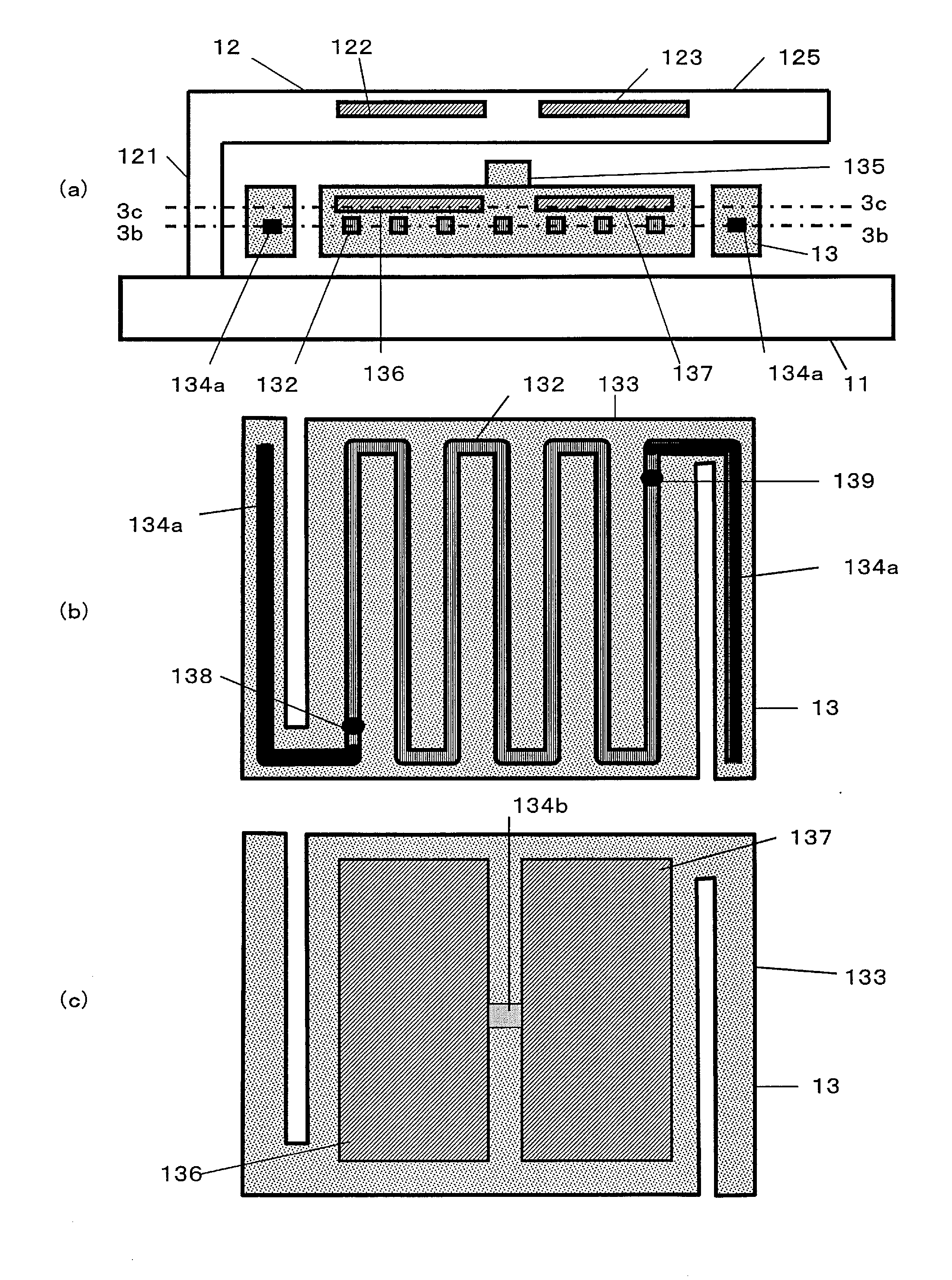
[0085]Hereinafter, a First Preferred Embodiment of an electronic device according to the present invention will be described with reference to the accompanying drawings. The electronic device of this preferred embodiment is an infrared sensor of a resistance changing type. However, the present invention is in no way limited to this specific preferred embodiment but is also applicable to a pyroelectric infrared sensor, a thermopile type infrared sensor, a dielectric bolometer type infrared sensor, or any other type of electronic device.

[0086]In this description, a section of an infrared sensor, of which a physical property changes with a variation in temperature and in which the quantity of the incident infrared radiation is detected based on that change will be referred to herein as an “infrared ray detecting section”. In an infrared sensor of the resistance changing type, for example, a bolometer made of a resistance changing material is the infrared ray detecting section. Meanwhil...

embodiment 2

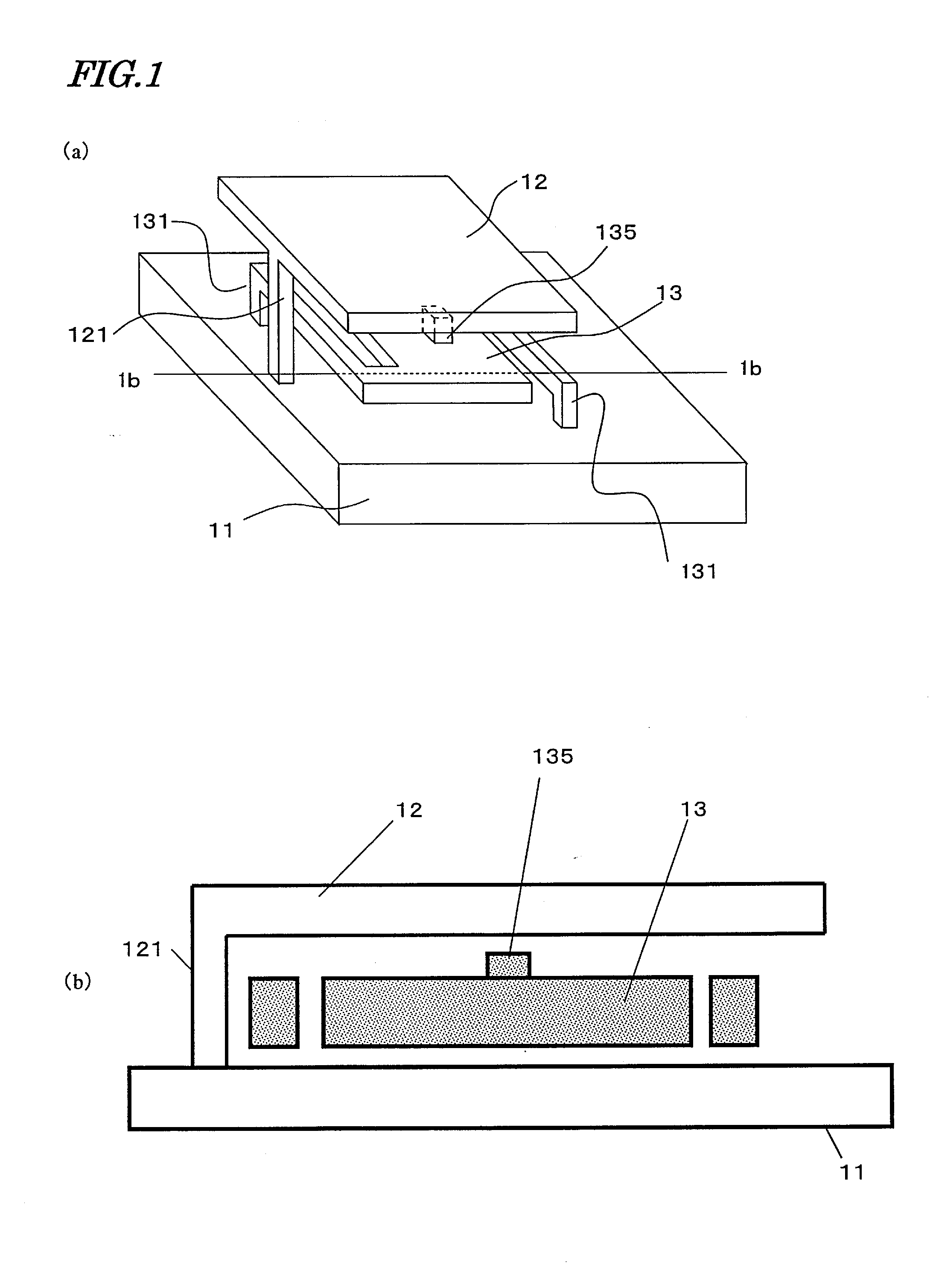
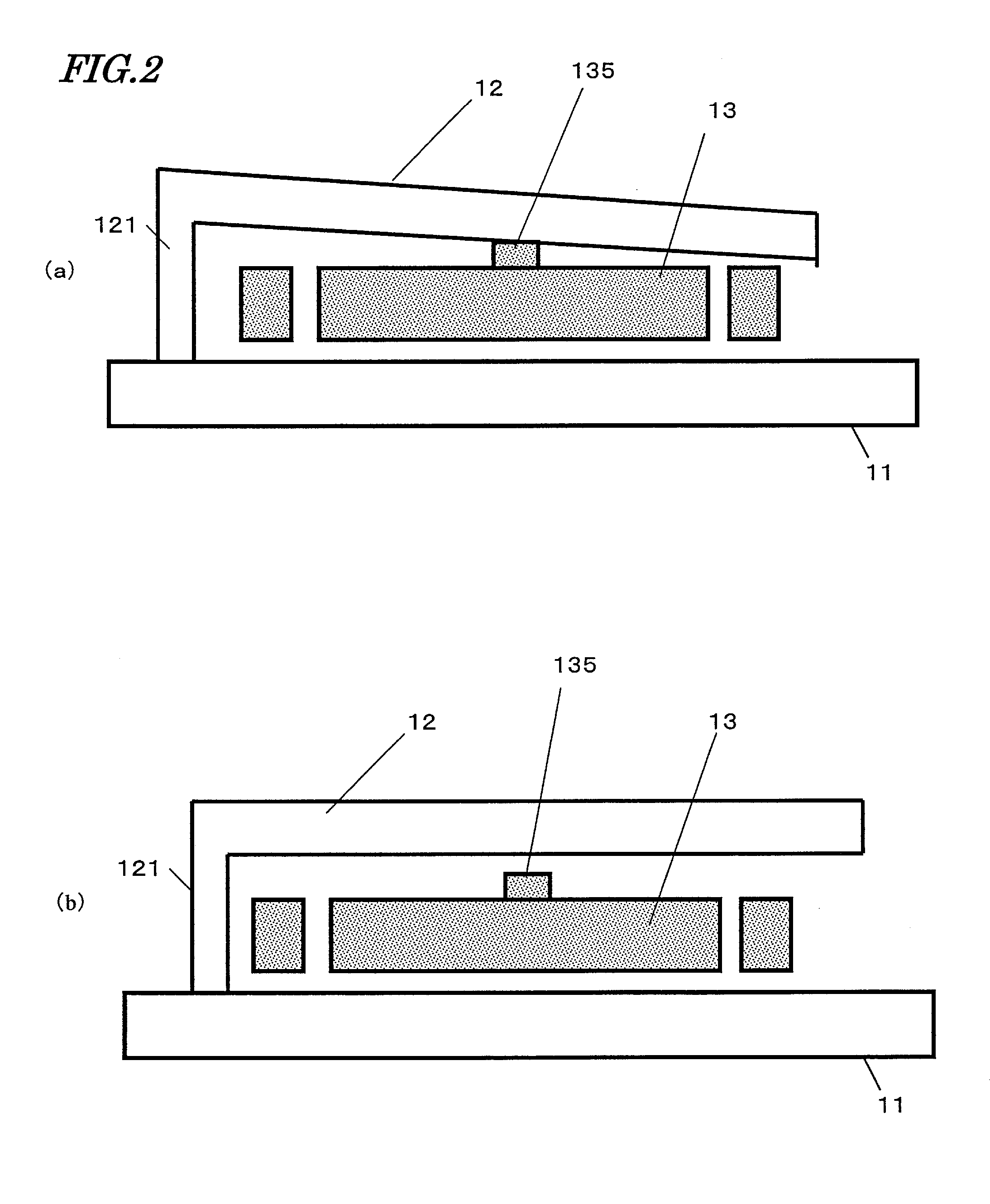
[0166]FIG. 11 illustrates an infrared sensor as another preferred embodiment of an electronic device according to the present invention. In this preferred embodiment, the infrared ray absorbing section 12 includes a first thermal contact portion 135a and the heat sensing section 13 includes a second thermal contact portion 135b. In this example, the first thermal contact portion 135a forms part of the infrared ray absorbing section 12 and the second thermal contact portion 135b forms part of the heat sensing section 13.

[0167]In this preferred embodiment, at least part of the first thermal contact portion 135a can either be deformed or shift thanks to the action of the driving section (not shown). That is why if at least part of the first thermal contact portion 135a is deformed or shift, the infrared ray absorbing section 12 and the heat sensing section 13 can make transitions between the in-contact and out-of-contact states as shown in FIGS. 11(a) and 11(b). For that reason, there ...


PUM


Abstract

An electronic device according to the present invention includes an infrared ray absorbing section 12, which comes to have an increased temperature when irradiated with an incident infrared ray, and at least one heat sensing section 13, of which a physical property varies with the variation in temperature that has been caused due to the heat generated by the infrared ray absorbing section 12. The relative positions of the heat sensing section 13 and the infrared ray absorbing section 12 can be changed so as to switch their states from a first state, in which the infrared ray absorbing section 12 and the heat sensing section 13 are in contact with each other, into a second state, in which the infrared ray absorbing section 12 and the heat sensing section 13 are out of contact with each other, and vice versa.

Description

TECHNICAL FIELD[0001]The present invention relates to an electronic device and more particularly relates to a thermal infrared sensor and a thermal infrared image sensor.BACKGROUND ART[0002]An infrared sensor for detecting an electromagnetic wave (or an infrared ray) with a wavelength of 3 μm to 10 μm has been used as a heat sensing sensor in crime prevention, measuring, remote sensing and various other fields of applications. An infrared image sensor, in which such sensors are arranged as a two-dimensional array, can obtain an even greater amount of information as a thermal image, and has been used extensively in those fields of applications.[0003]Infrared sensors are roughly classified into quantum sensors and thermal sensors. A quantum sensor is a sensor that is made of compound semiconductors and that operates by utilizing the band-to-band transition. Such a quantum sensor has higher sensitivity and higher response speed than a thermal sensor but operates at relatively low tempe...

Claims


Application Information

Patent Timeline
Patent Type & Authority Applications(United States)
IPC IPC(8): G01J5/02
CPCG01J5/02G01J5/023G01J5/0245G01J5/12G01J5/084G01J5/0853G01J5/08
Inventor IKUSHIMA, KIMIYA
Owner PANASONIC CORP
Why Eureka
Try Eureka