Ceramic electronic component and method for manufacturing the same

a ceramic electronic component and ceramic technology, applied in the direction of fixed capacitor details, stacked capacitors, fixed capacitors, etc., can solve the problems of reduced reliability, high cost, and high cost of electroless plating film, and achieve the effect of high effective volume and superior reliability

Active Publication Date: 2009-10-29
MURATA MFG CO LTD
View PDF17 Cites 12 Cited by
  • Summary
  • Abstract
  • Description
  • Claims
  • Application Information

AI Technical Summary

Benefits of technology

[0013]To overcome the problems described above, preferred embodiments of the present invention provide a ceramic electronic component having a high effective volume and superior reliability by forming external electrodes thereof only from plating films including glass particles, and a method for manufacturing the ceramic electronic component.

Problems solved by technology

However, with this method, a bonding force of the conductive metal layer formed by electroless plating to the side wall surface is weak, and reduced reliability may occur.
However, with the method for forming external electrodes disclosed in Japanese Unexamined Patent Application Publication No. 5-343259, since the plating method is electroless plating, depending on subsequent heat treatment conditions, blisters are likely to be generated in the electroless plating film.
When blisters are generated, moisture may enter therethrough, and problems, such as degradation in reliability, may arise.
Furthermore, with the above-described method for forming external electrodes, since the plating method is electroless plating, if it is attempted to co-deposit glass powder together with metal ions, there is a problem in that the glass is dissolved or is not sufficiently deposited.

Method used


Image

  • Ceramic electronic component and method for manufacturing the same
  • Ceramic electronic component and method for manufacturing the same
  • Ceramic electronic component and method for manufacturing the same

Examples


example 1

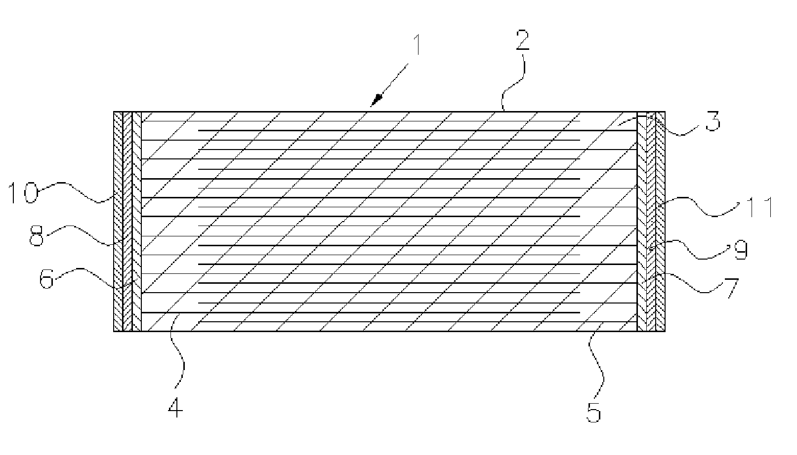
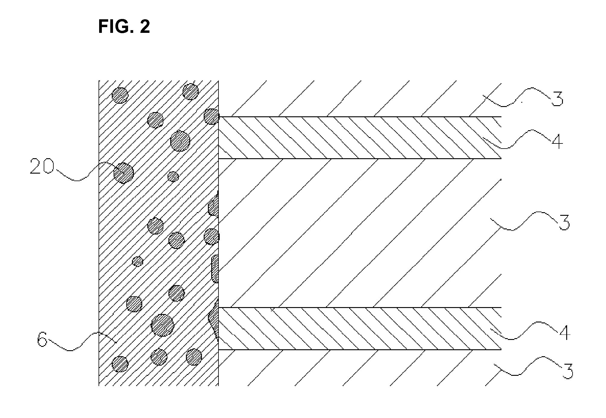
[0054]A laminate for a multilayer ceramic capacitor having a length of about 1.0 mm, a width of about 0.5 mm, and a thickness of about 0.5 mm was prepared. Dielectric layers were each formed from a barium titanate-based dielectric material, and internal electrodes were primarily formed of Ni. In addition, the thickness of the dielectric layer provided between adjacent internal electrodes was about 2 μm, and the thickness of the internal electrode was about 1 μm.

[0055]After the laminate was dried, a sand blasting treatment was performed using a polishing agent, so that an average protrusion length of the internal electrodes protruding from the surface of the laminate at which the internal electrodes were exposed was set to about 1 μm.

[0056]Next, a B—Si glass powder having a softening point of about 600° C. and an average particle diameter of about 1.1 μm was prepared. This glass powder was coated with an amino-based silane coupling agent.

[0057]The coated glass powder was added to a p...


PUM

PropertyMeasurementUnit
sizeaaaaaaaaaa
thicknessaaaaaaaaaa
lengthaaaaaaaaaa

Abstract

When external electrodes of a multilayer ceramic capacitor are formed by performing direct plating on surfaces at which internal electrodes are exposed without forming paste electrode layers, bonding forces of plating layers are relatively weak, and in addition, when glass particles are included in the plating layers, blisters are often generated. To overcome these problems, a multilayer ceramic capacitor is formed by performing electrolytic plating using a plating bath including glass particles, electrolytic plating layers including glass particles dispersed therein are formed as the external electrodes.

Description

BACKGROUND OF THE INVENTION[0001]1. Field of the Invention[0002]The present invention relates to a ceramic electronic component and a method for manufacturing the same, and more particularly, to external electrodes of a ceramic electronic component and a method for forming the external electrodes by an electrolytic plating method.[0003]2. Description of the Related Art[0004]A related multilayer ceramic capacitor includes a laminate which includes dielectric ceramic layers laminated to each other and layered internal electrodes provided along interfaces therebetween and external electrodes provided on the laminate so as to electrically connect the internal electrodes which are exposed on surfaces of the laminate. An example of this related multilayer ceramic capacitor is shown in FIG. 3.[0005]As shown in FIG. 3, external electrodes are provided on surfaces of a laminate 102 at which internal electrodes 104 and internal electrodes 105 are exposed so as to electrically connect the resp...

Claims


Application Information

Patent Timeline
Patent Type & Authority Applications(United States)
IPC IPC(8): H01G4/228B32B38/00C25D7/00
CPCC25D5/50C25D7/00H01G4/30H01G4/2325C25D15/00
Inventor OGAWA, MAKOTOMOTOKI, AKIHIRONAKAMURA, ICHIROYOSHIKAWA, NORIHIROIWANAGA, TOSHIYUKIKAWASAKI, KENICHITAKEUCHI, SHUNSUKE
Owner MURATA MFG CO LTD
Why Eureka
Try Eureka