Infrared detector, infrared detecting apparatus, and method of manufacturing infrared detector

a technology of infrared detectors and detectors, which is applied in the field of infrared detectors, can solve the problems of difficult growth of high-quality crystals, poor yield, and inability to obtain high-quality substrates with a large area, and achieves the effects of simple structure, improved detection sensitivity, and high efficiency

Active Publication Date: 2009-11-05
MITSUBISHI HEAVY IND LTD
View PDF6 Cites 15 Cited by
  • Summary
  • Abstract
  • Description
  • Claims
  • Application Information

AI Technical Summary

Benefits of technology

[0028]According to the first to the third aspects and according to the eleventh and the twelfth aspects of the present invention, photo-current is generated by the rays in the far-infrared range and in the middle-infrared range incident into the photo-current generating portion with what is known as a QWIP structure. The electrons of the photo-current thus generated are injected into the light emitting portion. The electrons thus injected and the holes are recombined so as to emit rays in the near-infrared range and in the visible range. The emitted rays in the near-infrared range and in the visible range are reflected by the reflection portion so as to be confined to the inside of the infrared detector. Then, the photo-detecting portion detects the emitted rays in the near-infrared range and in the visible range. Consequently, the infrared detector can achieve improvement in the detection sensitivity. In addition, the infrared detector is formed by forming the layers made of group III-V compound semiconductors on top of the substrate made of a group III-V compound semiconductor (for example, a GaAs substrate). Accordingly, an image sensor of a large area (a large number of pixels) can be obtained.
[0036]According to the tenth aspect of the present invention, the use of the infrared detector of the first aspect allows the infrared detecting apparatus to have high detection sensitivity and a large area (a large number of pixels).

Problems solved by technology

The infrared detectors made of HgCdTe can accomplish high quantum efficiency, but the low melting point and the high vapor pressure of Hg make the growth of a high-quality crystal difficult.
Manufacturing of HgCdTe image sensors results in an especially poor yield.
In addition, it is impossible to obtain a high-quality substrate (CdTe or the like) with a large area, and such unavailability makes it difficult to manufacture image sensors with a large number of pixels.
Accordingly, such image sensors are not sensitive to incident infrared rays from a direction that is perpendicular to the plane, which results in extremely low quantum efficiency.
The QWIPs that have been proposed thus far have not achieved satisfactory final detection sensitivity yet.
It is difficult, however, to manufacture an image sensor that can satisfy the above-mentioned two requirements.

Method used


Image

  • Infrared detector, infrared detecting apparatus, and method of manufacturing infrared detector
  • Infrared detector, infrared detecting apparatus, and method of manufacturing infrared detector
  • Infrared detector, infrared detecting apparatus, and method of manufacturing infrared detector

Examples


embodiment 1

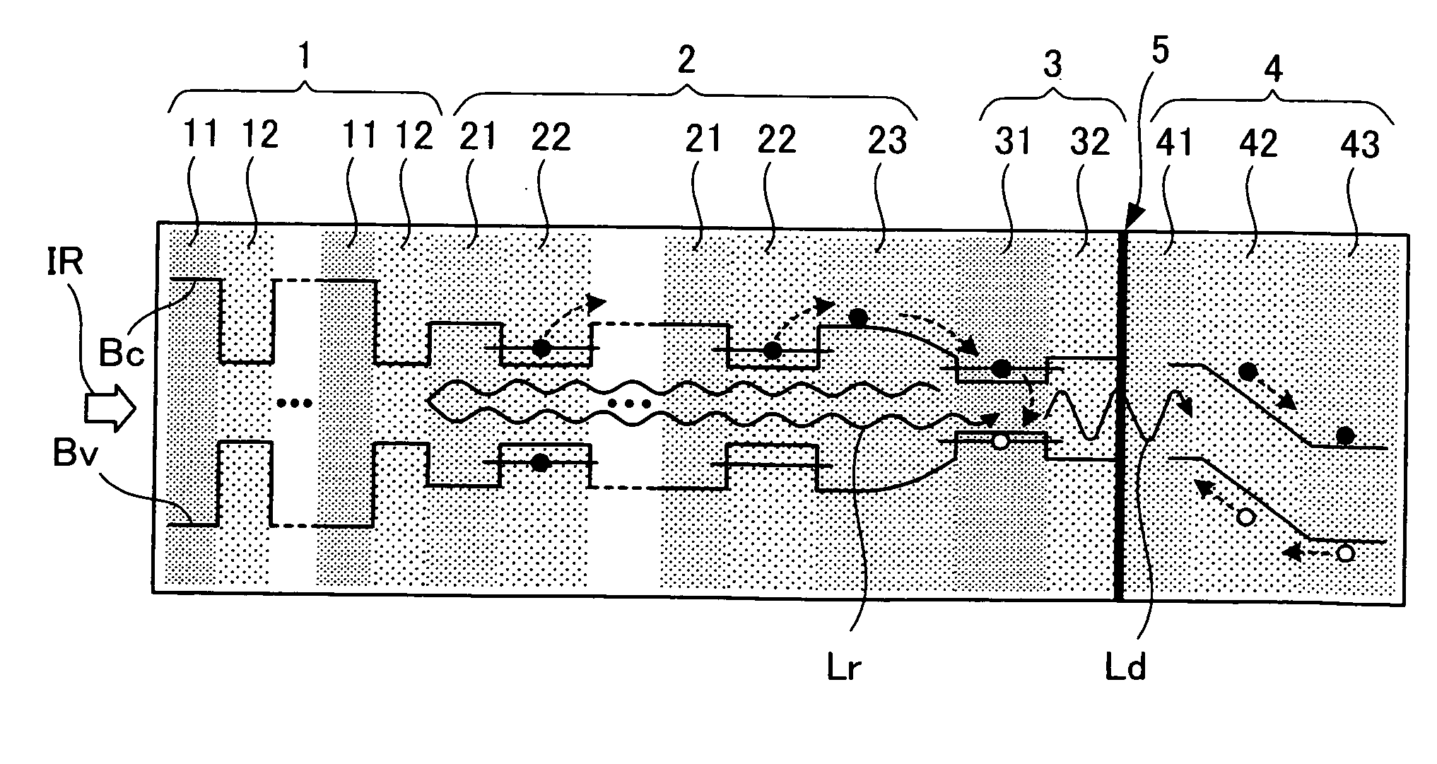
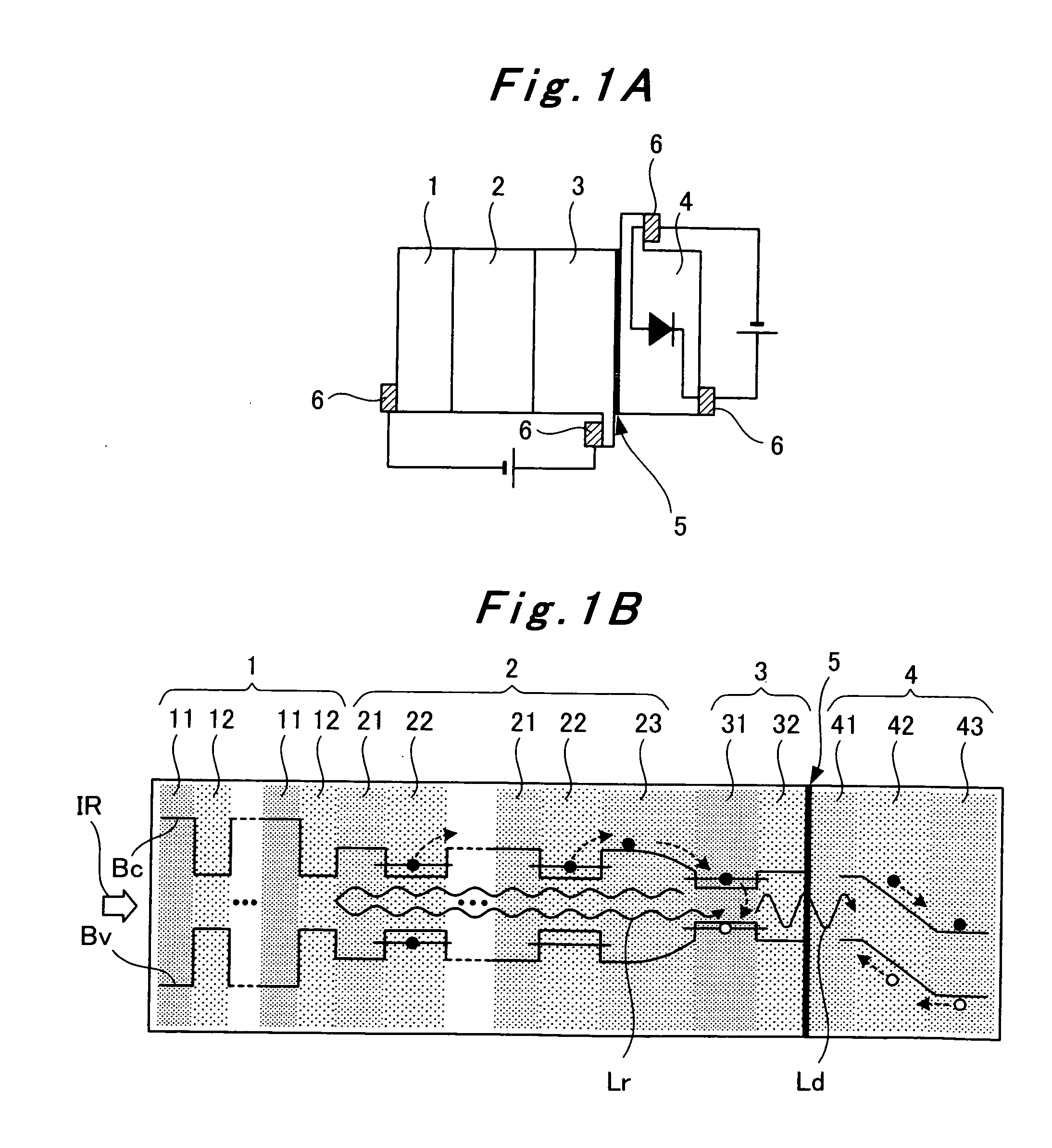
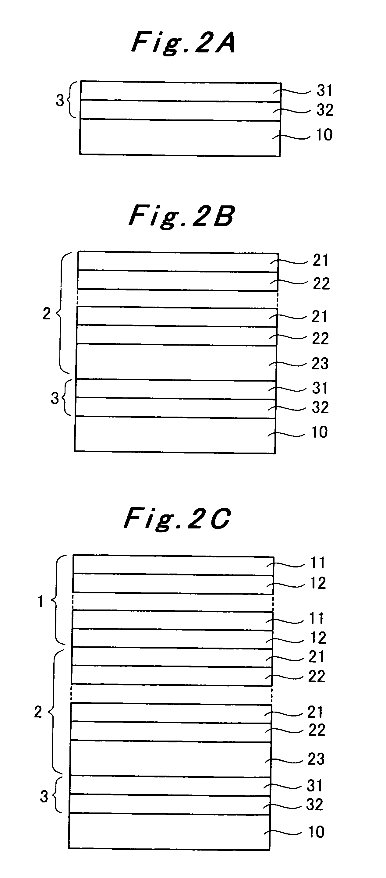
[0047]FIGS. 1A and 1B are diagrams describing an infrared detector according to a first embodiment of the present invention. FIG. 1A is a diagram describing, schematically, the configuration of the infrared detector. FIG. 1B is a diagram describing the structure of the infrared detector and the energy bands thereof. FIGS. 2A to 2C are diagrams describing a method of manufacturing the infrared detector.

[0048]As FIG. 1A illustrates, the infrared detector of Embodiment 1 includes a first element and a second element that are bonded together with a bonding portion 5 so as to form an integrated body. The first element includes a reflection portion 1, a photo-current generating portion 2, and a light emitting portion 3. The reflection portion 1 transmits rays in the far-infrared range and in the middle-infrared range, but reflects rays in the near-infrared range and in the visible range. The photo-current generating portion 2 has a multiple quantum well structure. In the multiple quantum ...

embodiment 2

[0082]FIGS. 4A and 4B are diagrams describing an infrared detector according to a second embodiment of the present invention. FIG. 4A is a diagram describing, schematically, the configuration of the infrared detector. FIG. 4B is a diagram describing the structure of the infrared detector and its energy bands. FIGS. 5A to D are diagrams describing a method of manufacturing the infrared detector. Note that in the following description those constituent elements of the infrared detector of Embodiment 2 that have their respective counterparts in the infrared detector of Embodiment 1 are denoted by the same reference numeral.

[0083]As FIG. 4A illustrates, the infrared detector of Embodiment 2 includes a reflection portion 1, a photo-current generating portion 2, a light emitting portion 3, and a photo-detecting portion 7. The reflection portion 1 transmits rays in the far-infrared range and in the middle-infrared range, but reflects rays in the near-infrared range and in the visible range...

embodiment 3

[0120]FIG. 6 is a diagram describing an infrared detector according to a third embodiment of the present invention. Note that the content of Embodiment 3 is implemented on the basis of the infrared detector of Embodiment 2, so that in the following description those constituent elements of the infrared detector of Embodiment 3 that have their respective counterparts in the infrared detector of Embodiment 2 are denoted by the same reference numeral. Needless to say, the content of Embodiment 3 can be implemented on the basis of the infrared detector of Embodiment 1.

[0121]As FIG. 6 illustrates, the infrared detector of Embodiment 3 includes a refraction layer 8 located on the incident surface side. The refraction layer 8 refracts the incident angle of the incident rays in the far-infrared range and in the middle-infrared range that enters perpendicularly the incident surface. Specifically, the refraction layer 8 made of GaAs is formed, firstly, through the crystal growth carried out b...


PUM


Abstract

An infrared detector comprises: a reflection portion transmitting far- and middle-infrared rays and reflecting near-infrared and visible rays; a photo-current generating portion having a quantum well structure in which electrons are excited by the far- and middle-infrared rays having passed through the reflection portion so as to generate photo-current; a light emitting portion having a quantum well structure into which electrons of the photo-current generated by the photo-current generating portion are injected and the electrons thus injected thereinto are recombined with holes, thus emitting near-infrared and visible rays; and a photo-detecting portion detecting the near-infrared and visible rays emitted from the light emitting portion, and detecting the near-infrared and visible rays emitted from the light emitting portion and reflected by the reflection portion. The reflection portion, the photo-current generating portion, and the light emitting portion are made of group III-V compound semiconductors layered on a semiconductor substrate.

Description

BACKGROUND OF THE INVENTION[0001]1. Field of the Invention[0002]The present invention relates to an infrared detector to detect infrared rays, an infrared detecting apparatus, and a method of manufacturing an infrared detector.[0003]2. Description of Related Art[0004]Among the infrared detectors that have been put to practical use, those detecting infrared rays in the far-infrared wavelength range (for example, a wavelength band ranging from 8 μm to 12 μm) include: infrared detectors made of a semiconductor of HgCdTe, which is a group II-VI compound; and quantum well infrared photo-detectors (QWIPs) made of a superlattice of a group III-V compound semiconductor (GaAs / AlGaAs).[0005]The infrared detectors made of HgCdTe can accomplish high quantum efficiency, but the low melting point and the high vapor pressure of Hg make the growth of a high-quality crystal difficult. Manufacturing of HgCdTe image sensors results in an especially poor yield. In addition, it is impossible to obtain a...

Claims


Application Information

Patent Timeline
Patent Type & Authority Applications(United States)
IPC IPC(8): H01L27/14H01L21/02
CPCB82Y20/00H01L31/02162H01L31/02322H01L31/0304Y02E10/544H01L31/107H01L31/125H01L31/184H01L31/035236Y02P70/50
Inventor KATO, MASAHIROMASUKAWA, KAZUNORIWATANABE, YOYAMAGUCHI, MASAHITOTANI, KOICHI
Owner MITSUBISHI HEAVY IND LTD
Why Eureka
Try Eureka