

Gallium nitride based compound semiconductor light-emitting device and method of manufacturing the same
a technology of compound semiconductors and light-emitting devices, which is applied in the direction of semiconductor/solid-state device manufacturing, semiconductor devices, electrical equipment, etc., can solve the problems of low emission power, difficult to obtain sufficient light emission efficiency, and difficult to emit light from the light-emitting device to the outside, so as to reduce the contact resistance between the p-type semiconductor layer and the transparent conductive oxide film , the effect of reducing the driving voltage v
- Summary
- Abstract
- Description
- Claims
- Application Information
AI Technical Summary
Benefits of technology
Problems solved by technology
Method used
Image

Examples
first embodiment
[0059]Hereinafter, a gallium nitride based compound semiconductor light-emitting device according to a first embodiment of the invention will be described with reference to FIGS. 1 to 4.
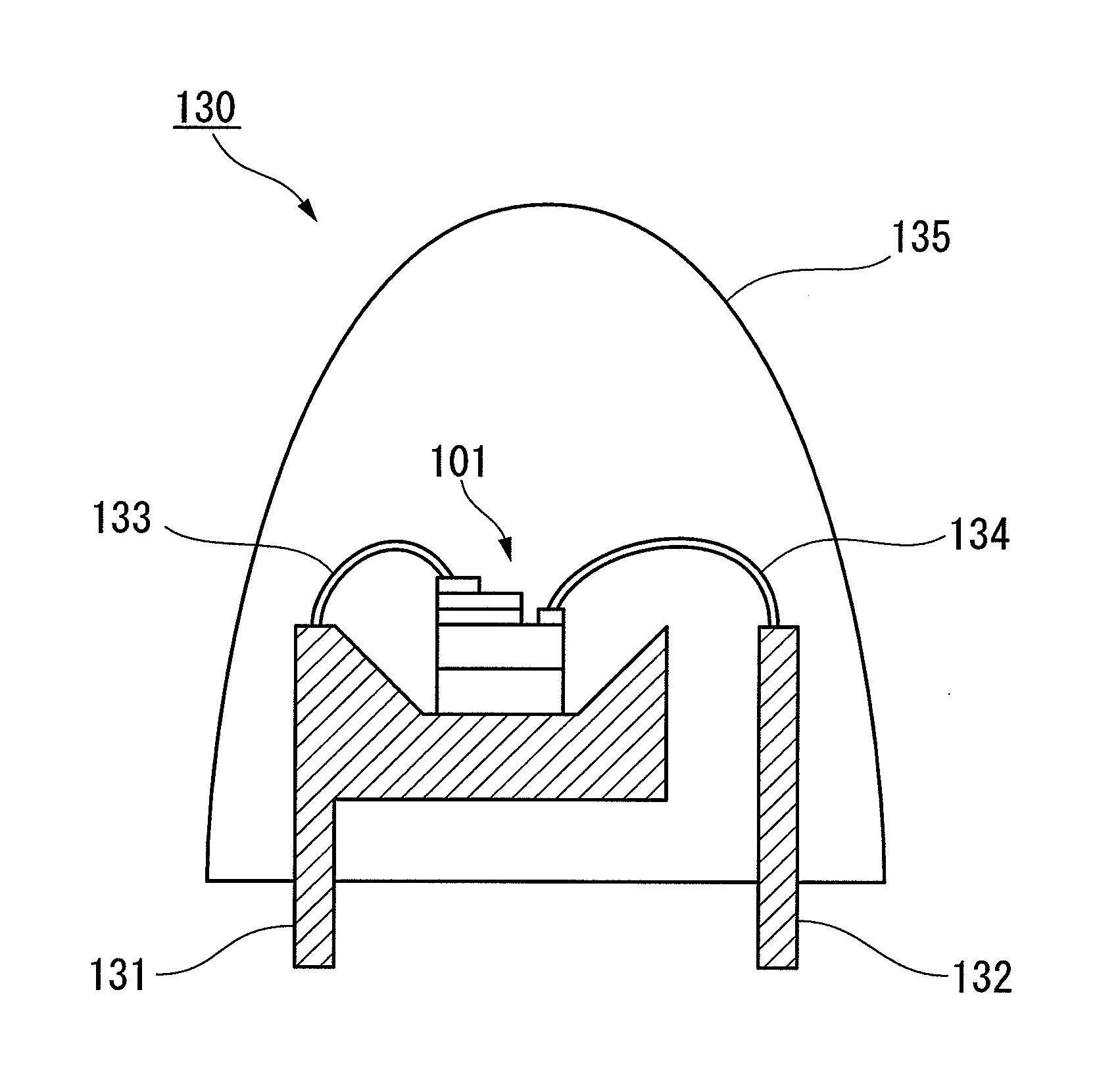
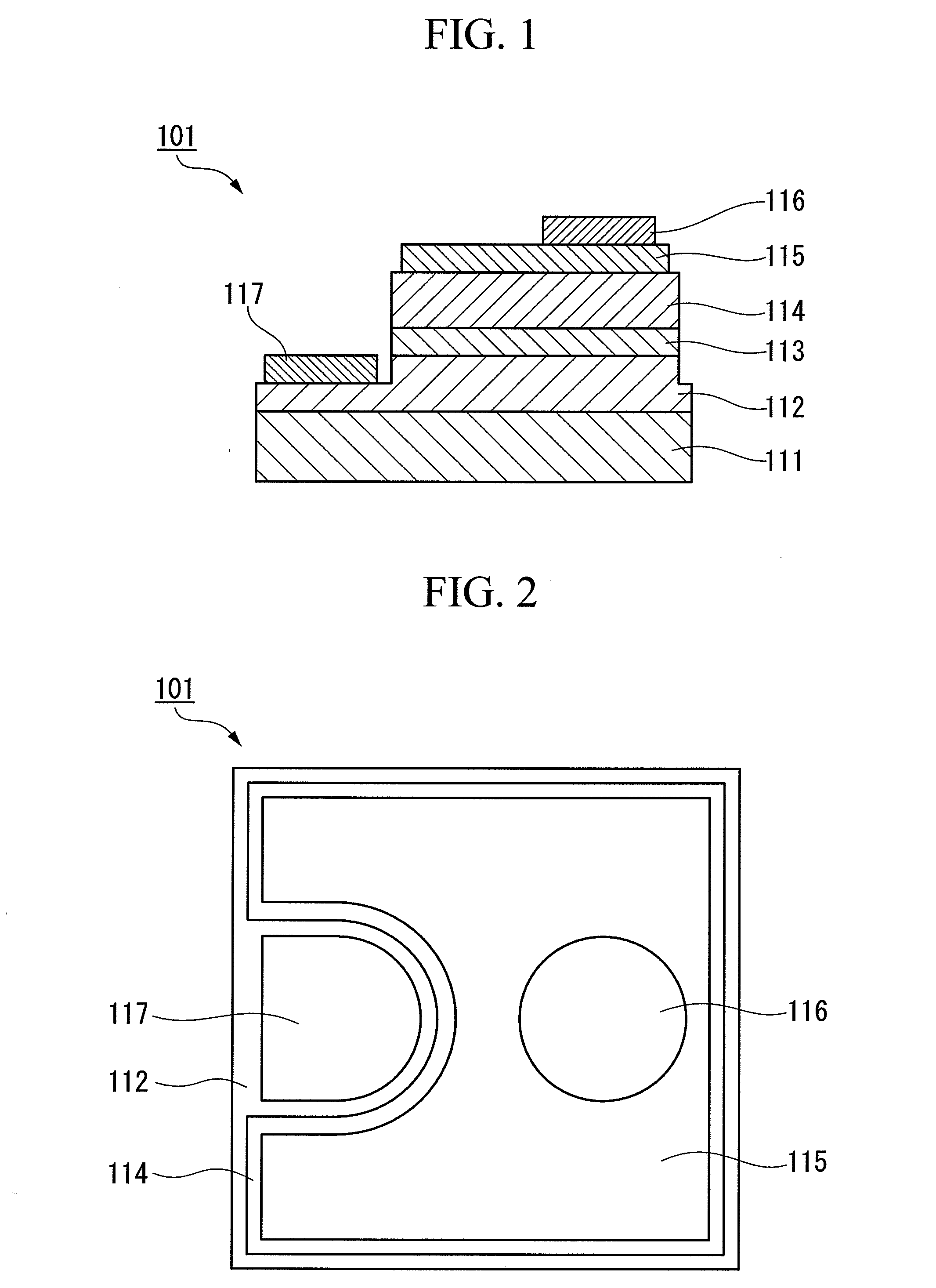
[0060]As shown in FIG. 1, a gallium nitride based compound semiconductor light-emitting device 101 according to this embodiment has a schematic structure in which an n-type GaN layer 112, a light-emitting layer 113, and a p-type GaN layer (p-type semiconductor layer) 114 are laminated on a substrate 111 in this order to form a gallium nitride based compound semiconductor device, a positive electrode 115 composed of a transparent conductive oxide film including dopants is formed on the p-type GaN layer 114 of the gallium nitride based compound semiconductor device, and the dopant concentration of an interface between the p-type GaN layer 114 and the positive electrode (transparent conductive oxide film) 115 is higher than the bulk dopant concentration of the transparent conductive oxide film forming t...
experimental example 1
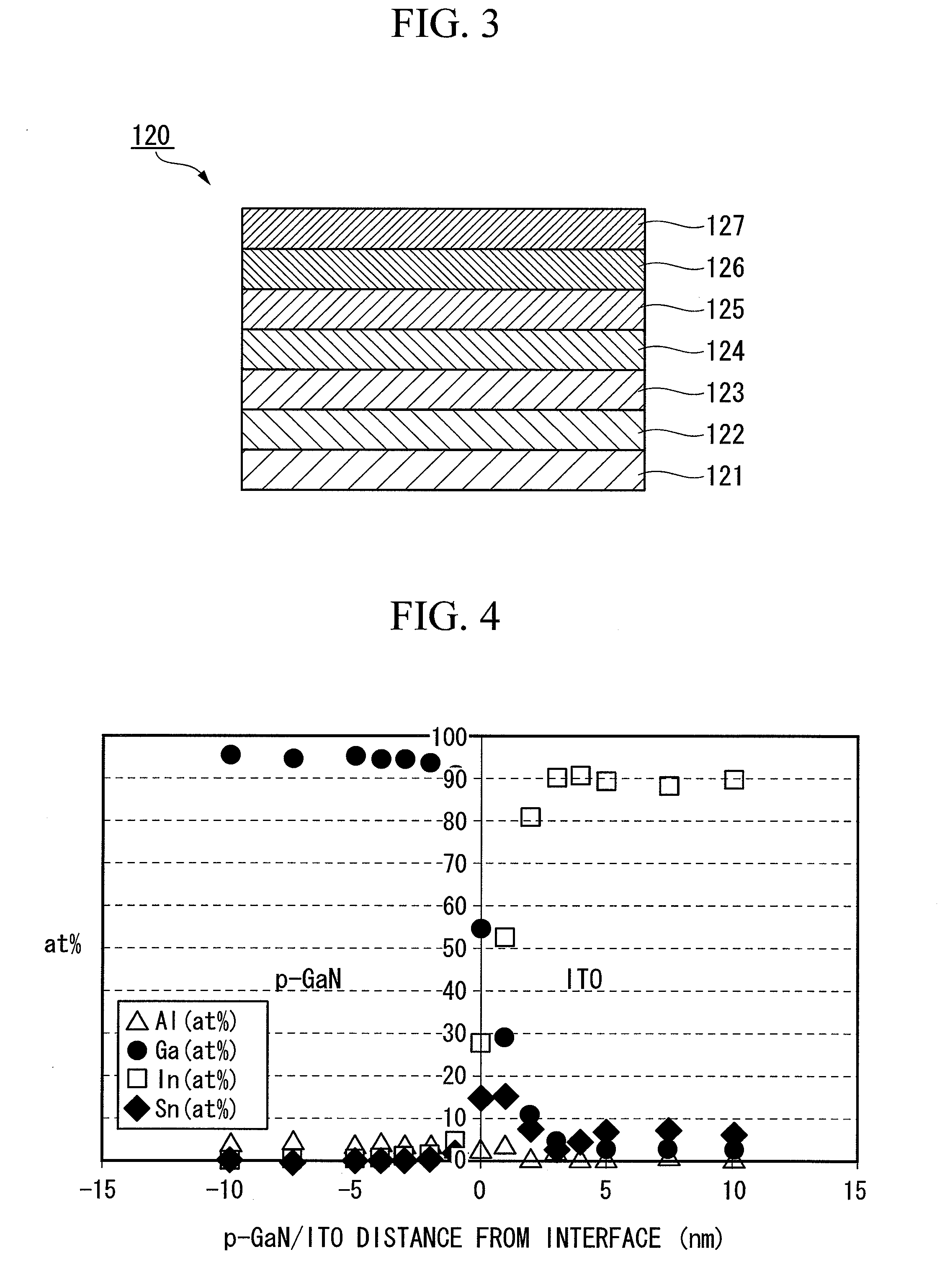
[0100]FIG. 3 is a cross-sectional view schematically illustrating an epitaxial structure used for the gallium nitride based compound semiconductor light-emitting device according to Examples of the invention. FIGS. 1 and 2 are respectively a cross-sectional view and a plan view schematically illustrating the gallium nitride based compound semiconductor light-emitting device according to the present invention. Next, the gallium nitride based compound semiconductor light-emitting device will be described with reference to FIGS. 1 to 3.
(Manufacture of Gallium Nitride Based Compound Semiconductor Light-Emitting Device)
[0101]The laminated structure of the gallium nitride based compound semiconductor light-emitting device 120 was formed by sequentially laminating, on a c-plane (0001) sapphire substrate 121, an undoped GaN underlying layer (thickness=2 μm) 122, a Si-doped n-type GaN contact layer (thickness=2 μm, and carrier concentration=1×1019 cm−3) 123, a Si-doped n-type Al0.07Ga0.93N c...
experimental examples 2 to 5
[0109]Before a transparent conductive oxide film layer made of ITO was formed, a transparent conductive oxide film contact layer with a thickness of about 2 nm was formed, and a gallium nitride based compound semiconductor light-emitting device was manufactured, similar to Experimental example 1.
PUM
| Property | Measurement | Unit |
|---|---|---|
| thickness | aaaaa | aaaaa |
| thickness | aaaaa | aaaaa |
| temperature | aaaaa | aaaaa |
Abstract
Description
Claims
Application Information