Method for making very low Vt metal-gate/high-k CMOSFETs using self-aligned low temperature shallow junctions

a low-temperature shallow junction and metal gate technology, applied in the direction of basic electric elements, electrical apparatus, semiconductor devices, etc., can solve the problems of undesirable high vsub>t/sub>, difficult choice of appropriate metal gate for p-mos, and reduced flat-band voltage (vsub>fb/sub>) of these devices, so as to reduce the defect-assisted diffusion and high mobility of 90

Inactive Publication Date: 2009-11-12
NAT CHIAO TUNG UNIV
View PDF3 Cites 3 Cited by
  • Summary
  • Abstract
  • Description
  • Claims
  • Application Information

AI Technical Summary

Benefits of technology

[0005]To overcome the drawbacks of the prior arts, this invention proposes a method to overcome these prior art's challenges. In this invention, at small 1.2 nm EOT, the self-aligned and gate-first [Ir—Hf] / HfLaO p- and n-MOS showed proper φm-eff of 5.3 and 4.1 eV, low Vt of +0.05 and 0.03 V, together with high mobility of 90 and 243 cm2 / Vs and good 85° C. reliability of small bias-temperature-instability (BTI). This good device performance was achieved by using a low-temperature (<900° C.) ultra-shallow junction (USJ) process, which lowers the interface reaction exponentially compared with a conventional 1000° C. RTA needed for ion-implantation dopant activation. The process temperature can even decrease to 650° C. for n-MOSFET using Ni / Sb SPD, where good device performances of low Vt of 0.14 V and mobility of 209 cm2 / Vs are still obtained. Besides, the measured USJ depth (Xj) was only 9.5˜20 nm for p+ / n case. The Xj for n+ / p was 23˜35 nm, better than that for a 1 keV As+ implant [7]* at the same sheet resistance (Rs). This is due to a reduction of defect-assisted diffusion arising from ion implant damage. These results compare well with previous work [1]*-[6]*, and display a lower Vt and smaller EOT, with a self-aligned USJ and gate-first process that is compatible with VLSI. This method included depositing HfLaO using PVD [1]*, a post-deposition anneal, and TaN / Ir and TaN / Hf deposition. After gate patterning, self-aligned 5 nm Ga or 10-nm-Ni / 5-nm-Ga (with top 100 nm SiO2 capping layer) was deposited for p-MOS, followed by 550˜900° C. RTA solid-phase diffusion (SPD). For n-MOS, self-aligned H3PO4 was spun deposited, transformed to P2O5 at 200° C. and SPD at 850˜900° C. RTA. Such wet H3PO4 spray and doping processes are used for commercial Si solar cell manufacture. Alternatively, the source-drain contact for n-MOS can be formed by 10-nm-Ni / 5-nm-Sb SPD at lower temperature of 600˜700° C. RTA. Finally, source-drain metal contacts were added. For comparison, [Ir3Si—HfxSi] / HfLaON CMOS using B+ and As+ implant and 1000° C. RTA were also fabricated.

Problems solved by technology

Although low-temperature-formed fully-silicidation (FUSI) of Lanthanide-silicide (YbxSi) [2]* and TaC gates work well for n-MOS, the choice of an appropriate metal gate for p-MOS is especially difficult.
Unfortunately, further scaling EOT to 1.2 nm, reduces flat-band voltage (Vfb) of these devices to produce an undesirable high Vt.
Since this approach was not successful, a fundamental understanding of the high Vt and Vfb roll-off is necessary, when EOT is scaled.

Method used


Image

  • Method for making very low Vt metal-gate/high-k CMOSFETs using self-aligned low temperature shallow junctions
  • Method for making very low Vt metal-gate/high-k CMOSFETs using self-aligned low temperature shallow junctions
  • Method for making very low Vt metal-gate/high-k CMOSFETs using self-aligned low temperature shallow junctions

Examples


Embodiment Construction

[0040]For the best understanding of this invention, please refer to the following detailed description of the preferred embodiments and the accompanying drawings.

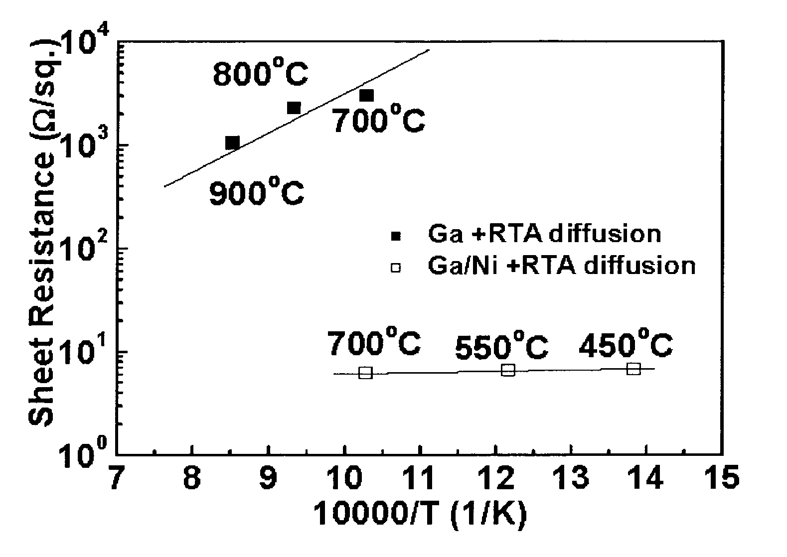
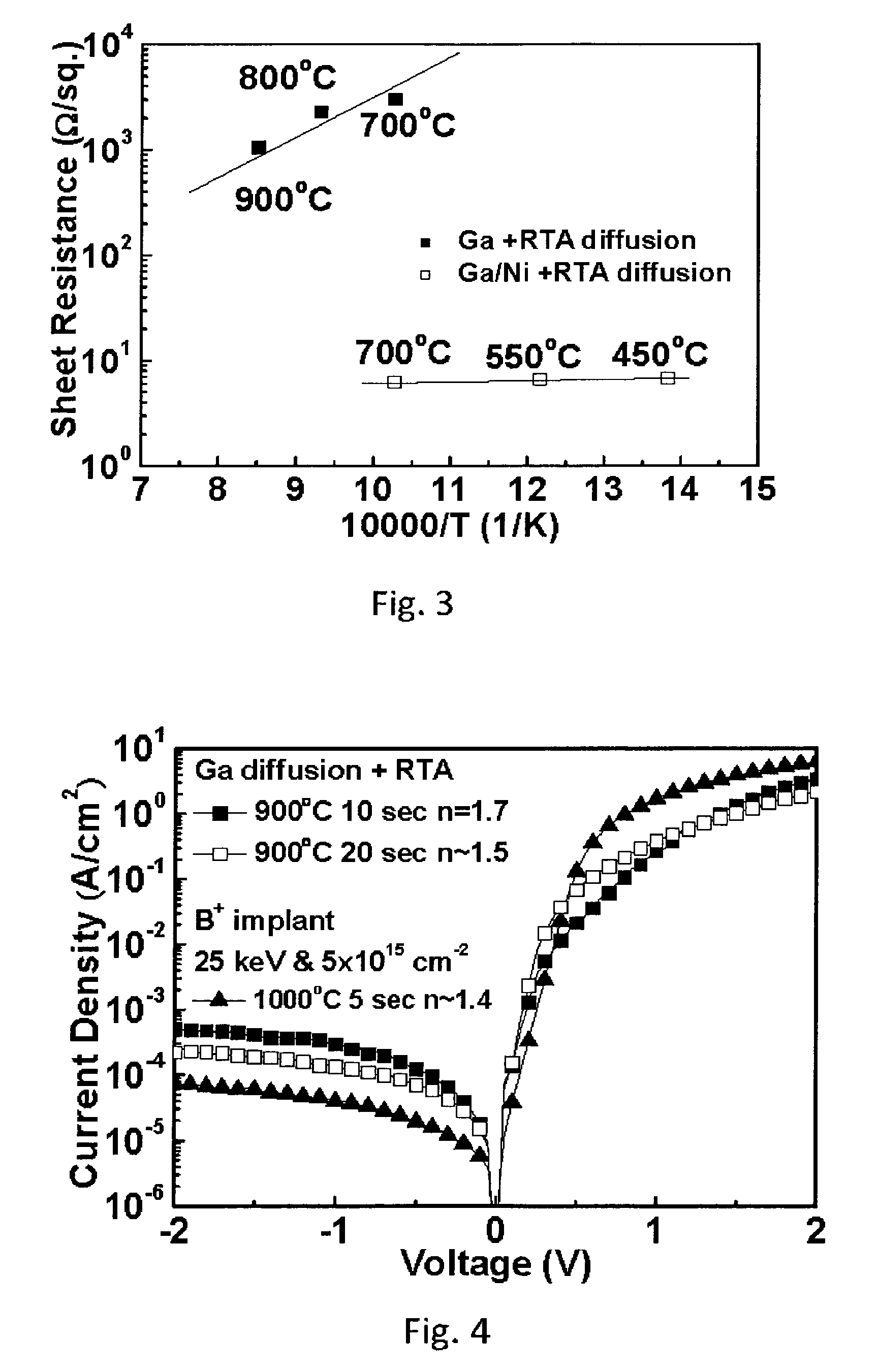
[0041]This invention proposes a method for making very low Vt metal-gate / high-κ CMOSFETs using self-aligned low temperature shallow junctions. The metal-gate / high-κ CMOSFETs process included depositing high-κ HfLaO using PVD [1]*, a post-deposition anneal, and TaN / Ir and TaN / Hf deposition. After gate patterning, self-aligned 5 nm Ga or 10-nm-Ni / 5-nm-Ga (with top 100 nm SiO2 capping layer) was deposited for p-MOS, followed by 550˜900° C. RTA solid-phase diffusion (SPD). For n-MOS, self-aligned H3PO4 was spun deposited, transformed to P2O5 at 200° C. and SPD at 850˜900° C. RTA. Such wet H3PO4 spray and doping processes are used for commercial Si solar cell manufacture. Alternatively, similar to p-MOS case, the source-drain contact of n-MOS can also be formed by Ni / Sb SPD at 600˜700° C. Finally, source-drain metal contacts wer...


PUM


Abstract

This invention proposes a method for making very low threshold voltage (Vt) metal-gate/high-κ CMOSFETs using novel self-aligned low-temperature ultra shallow junctions with gate-first process compatible with VLSI. At 1.2 nm equivalent-oxide thickness (EOT), good effective work-function of 5.3 and 4.1 eV, low Vt of +0.05 and 0.03 V, high mobility of 90 and 243 cm2/Vs, and small 85° C. bias-temperature-instability<32 mV (10 MV/cm, 1 hr) are measured for p- and n-MOS.

Description

BACKGROUND OF THE INVENTION [0001]1. Field of the Invention[0002]The invention relates to a method for making very low threshold voltage (Vt) metal-gate / high-κ CMOSFETs. More particularly, the invention relates to a method for making very Low Vt [Ir—Hf] / HfLaO CMOS using self-aligned low temperature shallow junctions with gate-first process compatible with VLSI fabrication process.[0003]2. Description of the Related Art[0004]The undesired high Vt at small equivalent-oxide thickness (EOT) is the major technology challenge for metal-gate / high-κ CMOSFETs, while the detailed mechanisms are still not clear yet [1]*-[6]* (please refer to table 1 for detail prior arts [1]*-[6]* listed in Summary of the Invention). One method to address this issue is to compensate the high Vt by using proper dual metal-gates, which have an effective work-function (φm-eff) lower than the target 4.1 eV for n-MOS, and higher than the needed 5.2 eV for p-MOS. Although low-temperature-formed fully-silicidation (F...

Claims


Application Information

Patent Timeline
Patent Type & Authority Applications(United States)
IPC IPC(8): H01L21/425
CPCH01L21/28088H01L21/823814H01L29/518H01L29/517H01L29/4966
Inventor CHIN, ALBERT
Owner NAT CHIAO TUNG UNIV
Why Eureka
Try Eureka