Tandem thin-film silicon solar cell and method for manufacturing the same

a technology of thin-film silicon and solar cells, which is applied in the manufacture of final products, pv power plants, radio frequency controlled devices, etc., can solve the problems of shortening the supply the production of solar-grade silicon wafers which is a main source, and the impact of energy on human future li

Inactive Publication Date: 2009-12-03
INTELLECTUAL DISCOVERY CO LTD
View PDF3 Cites 35 Cited by
  • Summary
  • Abstract
  • Description
  • Claims
  • Application Information

AI Technical Summary

Benefits of technology

[0023]In one aspect, a tandem thin-film silicon solar cell comprises a transparent substrate, a first unit cell positioned on the transparent substrate, the first unit cell comprising a p-type window layer, an i-type absorber layer and an n-type layer, an intermediate reflection layer positioned on the first unit cell, the intermediate reflection layer including a hydrogenated n-type microcrystalline silicon oxide of which the oxygen concentration is profiled to be gradually increased and a second unit cell positioned on the intermediate reflection layer, the second unit cell comprising a p-type window layer, an i-type absorber layer and an n-type layer.

Problems solved by technology

Recently, energy has become the most serious problem that impacts on human's future life due to the high oil price and the global warming caused by an excessive emission of CO2.
However, production of solar-grade silicon wafer which is a main source does not catch up with explosive demand, and the solar-grade silicon wafer is running short all over the world.
However, the so-called Staebler-Wronski effect is blocking the commercialization of the thin-film silicon solar cells.
Meanwhile, although the degradation against light soaking is reduced, there is a limit to performance achieved by single-junction thin-film silicon solar cells.
However, in mass production of large-area solar cells, problems such as shunts are generated in zinc oxide when the zinc oxide intermediate reflection layer is patterned through laser scribing.

Method used


Image

  • Tandem thin-film silicon solar cell and method for manufacturing the same
  • Tandem thin-film silicon solar cell and method for manufacturing the same
  • Tandem thin-film silicon solar cell and method for manufacturing the same

Examples


Embodiment Construction

[0046]Reference will now be made in detail embodiments of the invention examples of which are illustrated in the accompanying drawings.

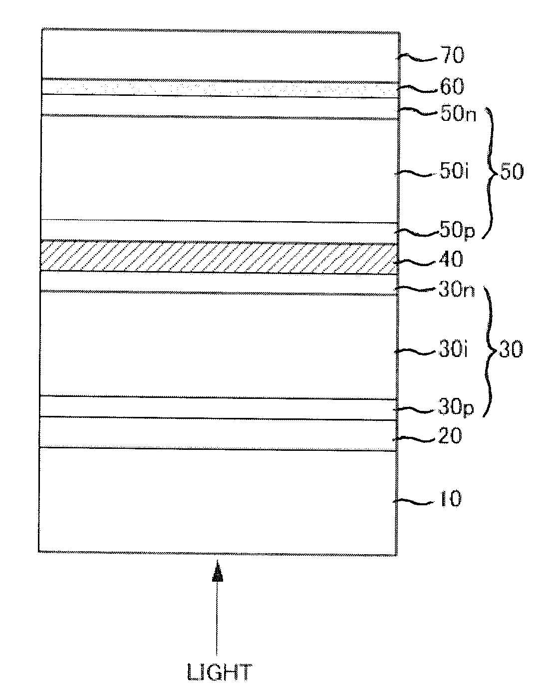
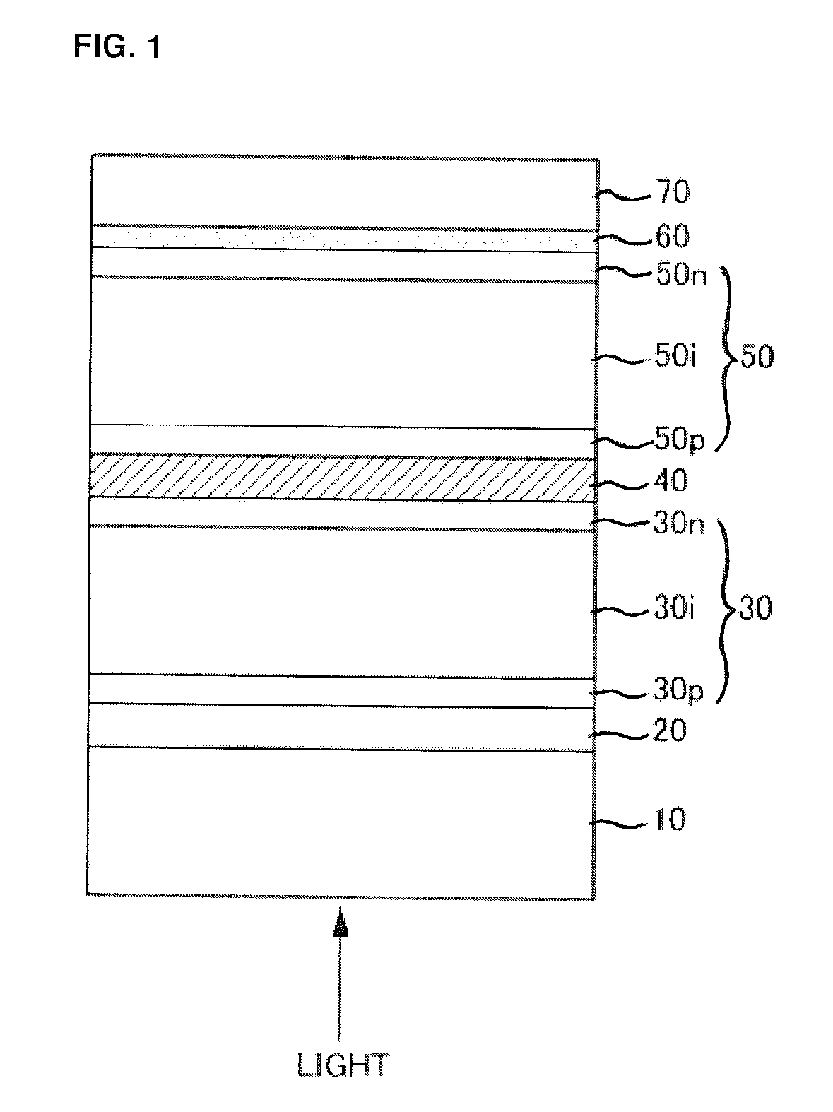
[0047]Tandem thin-film silicon solar cell has a double-junction structure or a triple-junction structure. However, a tandem thin-film silicon solar cell having a double-junction structure will be described as an example in FIG. 1.

[0048]As illustrated in FIG. 1, a tandem thin-film silicon solar cell according to an embodiment comprises a transparent insulating substrate 10, a transparent front electrode 20, a first unit cell 30, an intermediate reflection layer 40, a second unit cell 50 and a metal rear electrode 70.

[0049]The transparent front electrode 20 is formed on the transparent insulating substrate 10 and includes a transparent conducting oxide (TCO).

[0050]The first unit cell 30 are positioned on the transparent insulating substrate 10 and the transparent front electrode 20 and comprises a p-type window layer 30p, an i-type absorber layer 30i a...


PUM


Abstract

A tandem thin-film silicon solar cell comprises a transparent substrate, a first unit cell positioned on the transparent substrate, the first unit cell comprising a p-type window layer, an i-type absorber layer and an n-type layer, an intermediate reflection layer positioned on the first unit cell, the intermediate reflection layer including a hydrogenated n-type microcrystalline silicon oxide of which the oxygen concentration is profiled to be gradually increased and a second unit cell positioned on the intermediate reflection layer, the second unit cell comprising a p-type window layer, an i-type absorber layer and an n-type layer.

Description

[0001]This application claims the benefit of Korean Patent Application No. 10-2008-0049000 filed on May 27, 2008 which is hereby incorporated by reference.BACKGROUND[0002]1. Field[0003]The present embodiment relates to a tandem thin-film silicon solar cell and a method for manufacturing the same.[0004]2. Description of the Related Art[0005]Recently, energy has become the most serious problem that impacts on human's future life due to the high oil price and the global warming caused by an excessive emission of CO2. Many technologies for renewable energy have been developed, such as wind power generation, bio-energy, hydrogen fuel cells and the like. However, solar energy is almost infinite and clean energy as the origin of all energies, and hence solar cells using sunlight have become into the spotlight.[0006]The power of sunlight incident on the surface of the earth is 120,00 TW. Theoretically, if only 0.16% of the surface area of land on the earth is covered with solar cells having...

Claims


Application Information

Patent Timeline
Patent Type & Authority Applications(United States)
IPC IPC(8): H01L31/052H01L31/18H01L31/076
CPCH01L31/02167H01L31/03685H01L31/03687H01L31/076Y02E10/547Y02E10/548Y02E10/545H01L31/1804Y02E10/52Y02P70/50H01L31/075H01L31/18H01L31/0445H01L31/047
Inventor MYONG, SEUNG-YEOP
Owner INTELLECTUAL DISCOVERY CO LTD
Why Eureka
Try Eureka