

Intermediate multilayer wiring board product, and method for manufacturing multilayer wiring board
a multi-layer wiring board and intermediate technology, applied in the direction of printed circuit aspects, printed circuit components, semiconductor/solid-state device details, etc., can solve the problems of deteriorating the yield of multi-layer wiring boards, insufficient strength of intermediate multi-layer wiring boards, and insufficient strength of coreless wiring boards, so as to reduce resistance of metal foils, shorten the process of manufacturing multi-layer wiring boards, and enhance the conductivity of metal foils
- Summary
- Abstract
- Description
- Claims
- Application Information
AI Technical Summary
Benefits of technology
Problems solved by technology
Method used
Image

Examples
first exemplary embodiment
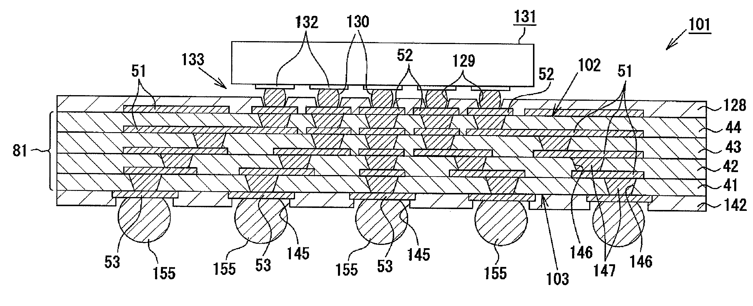
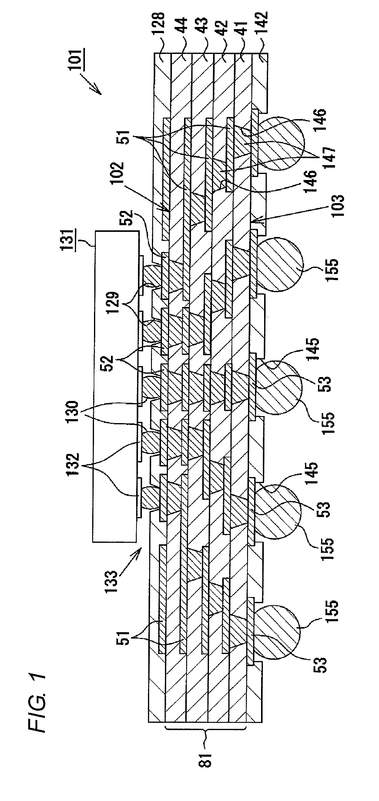
[0070]FIG. 1 is a cross-sectional view showing a coreless wiring board 101 (a multilayer wiring board) of one exemplary embodiment. The coreless wiring board 101 is a wiring board that does not have any core board and that has a structure made by alternately stacking a conductor layer 51 made of copper and four resin insulating layers 41, 42, 43, and 44 made of an epoxy resin. The resin insulating layers 41 to 44 are intermediate insulating layers that have the same thickness and that are made of the same material (i.e., the resin insulating layers 41 to 44 are of a same type a resin insulating layer).
[0071]Terminal pads 52 are arranged in an arrayed pattern on a front surface 102 (a surface of a resin insulating layer 44 on the fourth stratum counted from bottom layer 41 of the stack of the resin insulating layers 41-44) of the coreless wiring board 101. Further, the substantially entire surface of the resin insulating layer 44 is covered with a solder resist 128. Openings 129 for ...
second exemplary embodiment
[0097]A second exemplary embodiment of the invention will be described with reference to drawings. In the second exemplary embodiment, non-formation regions are formed on an intermediate product, instead of the cut portions 61 of the first exemplary embodiment. Similar or identical elements and operations in connection with the first exemplary embodiment are denoted by identical reference symbols, and the description thereof is omitted in this exemplary embodiment.
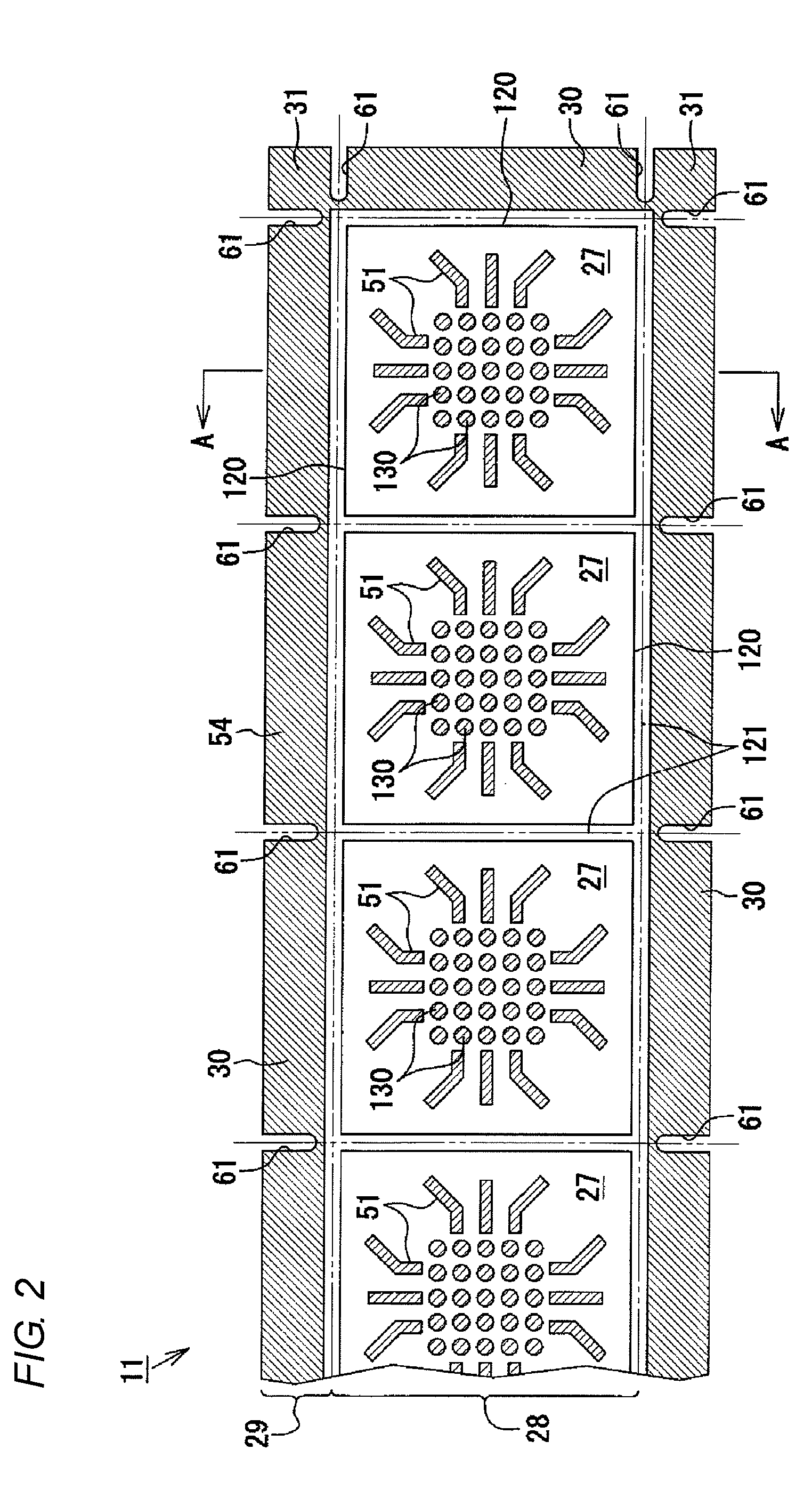
[0098]FIG. 17 is a schematic plan view showing an intermediate product 12 of a coreless wiring board according to the second exemplary embodiment. Since a cross-sectional view of the coreless wiring board of this exemplary embodiment is the same as that shown in FIG. 1, and a cross-sectional view of the intermediate product 12 cut along A-A line of FIG. 17 is the same as that shown in FIG. 3, related description thereto is omitted.
[0099]As shown in FIG. 17, a plurality of non-formation regions 62 are arranged on each of th...
PUM
| Property | Measurement | Unit |
|---|---|---|
| Thickness | aaaaa | aaaaa |
| Ratio | aaaaa | aaaaa |
| Width | aaaaa | aaaaa |
Abstract
Description
Claims
Application Information